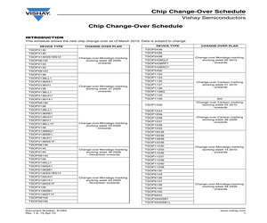
TSOP4838SI1 TSOP2233 TSOP4838SJ1 TSOP2233LL1 TSOP4838SK1AM TSOP2233UH1 TSOP2233VI1 TSOP4833 Change-over Mondego marking working week 03 2009 - January onwards TSOP4838SO1 TSOP4838SP1 TSOP4838SS1BS12Z TSOP58233 TSOP4838SS1F TSOP2236 TSOP4838ST1 TSOP2236AY1 TSOP4838UH1 TSOP2236KU1 TSOP4838VI1 TSOP2236LL1 TSOP4838YA1 TSOP2236QJ1 TSOP4838UH1B TSOP2236RF1 TSOP4838LL1B TSOP2236SA1 TSOP4838YA1B TSOP2236SJ1 TSOP58238 TSOP2236SP1 TSOP2240 TSOP2236UH1 TSOP2240RF1 TSOP2236VI1 TSOP4840 TSOP2236YA1 TSOP4840SB1 TSOP4836 TSOP4840SI1 TSOP4836LL1 TSOP4840SJ1 TSOP4836SB1 TSOP58240 TSOP4836ST1 TSOP4836UH1 Change-over Mondego marking working week 44 2008 - November onwards Change-over Mondego marking working week 44 2008 - November onwards TSOP4838SS1BS12 TSOP4833SS1BS12Z TSOP4836SI1 CHANGE-OVER PLAN Change-over Mondego marking working week 16 2009 - onwards TSOP2256 TSOP2256IV1 TSOP2256SB1 TSOP4836YA1 TSOP2256YA1 TSOP4836LL1B TSOP4856 TSOP4836SS1F TSOP4856SB1 TSOP58236 TSOP58256 Change-over Mondego mar
 2 Pages, 19 KB, Original
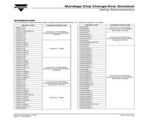
P4838AY1 TSOP4838DA1 TSOP4838LL1 TSOP4838QJ1 TSOP4838RF1 TSOP4838SB1 TSOP4838SI1 TSOP4838SJ1 TSOP4838SK1AM TSOP4838SO1 TSOP4838SP1 Changed over Mondego marking working week 44 2008 November onwards TSOP4838SS1BS12 TSOP4838SS1BS12Z TSOP4838SS1F TSOP4838ST1 TSOP4838UH1 TSOP4838VI1 TSOP4838YA1 TSOP4838UH1B TSOP4838LL1B TSOP4838YA1B TSOP58238 TSOP2240 TSOP2240RF1 TSOP4840 TSOP4840SB1 Quarter 2 - 2009 TSOP4840SI1 TSOP4840SJ1 TSOP58240 TSOP2256 TSOP2256IV1 TSOP2256SB1 TSOP2256YA1 TSOP4856 Changed over Mondego marking working week 40 2008 October onwards TSOP4856SB1 TSOP58256 www.vishay.com 2 Document Number: 81594 Rev. 1.1, 23-Feb-09
 2 Pages, 16 KB, Original
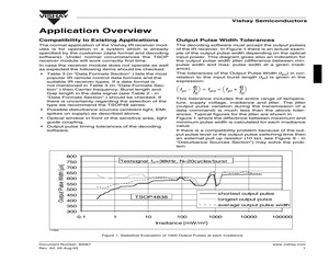
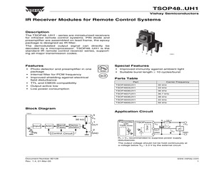
TSOP4838UH1 TSOP4856UH1 fo 30 kHz 36 kHz 38 kHz 56 kHz Type TSOP4833UH1 TSOP4837UH1 TSOP4840UH1 fo 33 kHz 36.7 kHz 40 kHz Description The TSOP48..UH1 - series are miniaturized receivers for infrared remote control systems. PIN diode and preamplifier are assembled on lead frame, the epoxy package is designed as IR filter. The demodulated output signal can directly be decoded by a microprocessor. TSOP48..UH1 is the standard IR remote control receiver series, supporting all major transmission codes. 16 081 Features D Photo detector and preamplifier in one package D Internal filter for PCM frequency D Improved shielding against electrical field D Low power consumption D High immunity against ambient light D Continuous data transmission possible (800 bit/s) disturbance D Suitable burst length 10 cycles/burst D TTL and CMOS compatibility D Output active low Block Diagram 3 Control Circuit Input 30 k W 1 PIN AGC Band Pass VS OUT Demodulator 2 GND 9612226 Document Number 82128 Rev. 3, 29-Mar-01 www.visha
 7 Pages, 159 KB, Original
Battery-Powered Systems There are two main limitations using the IR receiver modules in a battery-powered system: The supply voltage range and the supply current. Document Number: 80067 Rev. A2, 05-Aug-03 All standard types with 4 digits (e.g. TSOP4838 or TSOP4838UH1) are designed for a supply voltage range between 4.5 V and 5.5 V. All types with 5 digits and with the first digit as a ''3'' (e.g. TSOP34838) are designed for a supply voltage range between 2.7 V and 5.5 V. If the operating temperature is limited to a range between 0 C and + 60 C then it can even work down to 2.3 V. A supply current of approximately 1.2 mA is too much for continuous operation at a normal battery. If the power supply cannot be turned off, because stand-by reception of IR signals is required, then a pulsed supply voltage can help to save battery power. In this case the supply voltage can be turned on repetitively for a short duration as shown in Figure 4. If the IR receiver can sense a signal in this time window then
 6 Pages, 92 KB, Original
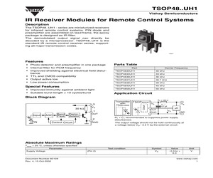
compatibility * Output active low * Low power consumption * Improved immunity against ambient light * Suitable burst length 10 cycles/burst e3 Parts Table Part Carrier Frequency TSOP4830UH1 30 kHz TSOP4833UH1 33 kHz TSOP4836UH1 36 kHz TSOP4837UH1 36.7 kHz TSOP4838UH1 38 kHz TSOP4840UH1 40 kHz TSOP4856UH1 56 kHz Block Diagram Application Circuit 16833 3 16842 1 Input AGC Band Pass Demodulator OUT 2 PIN Control Circuit GND Transmitter TSOPxxxx with TSALxxxx Circuit 30 k VS R1 = 100 VS OUT GND +VS C1 = 4.7 F C VO GND R1 + C1 recommended to suppress power supply disturbances. The output voltage should not be hold continuously at a voltage below VO = 3.3 V by the external circuit. Document Number 82128 Rev. 1.4, 01-Mar-05 www.vishay.com 1 TSOP48..UH1 Vishay Semiconductors Absolute Maximum Ratings Absolute Maximum Ratings Tamb = 25 C, unless otherwise specified Symbol Value Supply Voltage Parameter (Pin 2) Test condition VS - 0.3 to + 6.0 V Supply Current (Pin 2) IS 5 mA Output Voltage (Pin 1) VO - 0.3
 8 Pages, 258 KB, Original
TSOP4838UH1 TSOP4856UH1 fo 30 kHz 36 kHz 38 kHz 56 kHz Type TSOP4833UH1 TSOP4837UH1 TSOP4840UH1 fo 33 kHz 36.7 kHz 40 kHz Description The TSOP48..UH1 - series are miniaturized receivers for infrared remote control systems. PIN diode and preamplifier are assembled on lead frame, the epoxy package is designed as IR filter. The demodulated output signal can directly be decoded by a microprocessor. TSOP48..UH1 is the standard IR remote control receiver series, supporting all major transmission codes. 16 081 Features D Photo detector and preamplifier in one package D Internal filter for PCM frequency D Improved shielding against electrical field D Low power consumption D High immunity against ambient light D Continuous data transmission possible (800 bit/s) disturbance D Suitable burst length 10 cycles/burst D TTL and CMOS compatibility D Output active low Block Diagram 3 Control Circuit Input 30 kW 1 PIN AGC Band Pass VS OUT Demodulator 2 GND 9612226 Document Number 82128 Rev. 1, 26-Apr-00 www.vishay
 7 Pages, 113 KB, Original
TSOP4838UH1 TSOP4856UH1 fo 30 kHz 36 kHz 38 kHz 56 kHz Type TSOP4833UH1 TSOP4837UH1 TSOP4840UH1 fo 33 kHz 36.7 kHz 40 kHz Description The TSOP48..UH1 - series are miniaturized receivers for infrared remote control systems. PIN diode and preamplifier are assembled on lead frame, the epoxy package is designed as IR filter. The demodulated output signal can directly be decoded by a microprocessor. TSOP48..UH1 is the standard IR remote control receiver series, supporting all major transmission codes. 16 081 Features D Photo detector and preamplifier in one package D Internal filter for PCM frequency D Improved shielding against electrical field D Low power consumption D High immunity against ambient light D Continuous data transmission possible (800 bit/s) disturbance D Suitable burst length 10 cycles/burst D TTL and CMOS compatibility D Output active low Block Diagram 3 Control Circuit Input 30 kW 1 PIN AGC Band Pass VS OUT Demodulator 2 GND 9612226 Document Number 82128 Rev. 3, 29-Mar-01 www.vishay
 7 Pages, 156 KB, Original
compatibility * Output active low * Low power consumption * Improved immunity against ambient light * Suitable burst length 10 cycles/burst e3 Parts Table Part Carrier Frequency TSOP4830UH1 30 kHz TSOP4833UH1 33 kHz TSOP4836UH1 36 kHz TSOP4837UH1 36.7 kHz TSOP4838UH1 38 kHz TSOP4840UH1 40 kHz TSOP4856UH1 56 kHz Block Diagram Application Circuit 16833 3 16842 1 Input AGC Band Pass Demodulator OUT 2 PIN Control Circuit GND Transmitter TSOPxxxx with TSALxxxx Circuit 30 k VS R1 = 100 VS OUT GND +VS C1 = 4.7 F C VO GND R1 + C1 recommended to suppress power supply disturbances. The output voltage should not be hold continuously at a voltage below VO = 3.3 V by the external circuit. Document Number 82128 Rev. 1.4, 01-Mar-05 www.vishay.com 1 TSOP48..UH1 Vishay Semiconductors Absolute Maximum Ratings Absolute Maximum Ratings Tamb = 25 C, unless otherwise specified Symbol Value Supply Voltage Parameter (Pin 2) Test condition VS - 0.3 to + 6.0 V Supply Current (Pin 2) IS 5 mA Output Voltage (Pin 1) VO - 0.3
 7 Pages, 232 KB, Original
* Output active low * Low power consumption Special Features * Improved immunity against ambient light * Suitable burst length 10 cycles/burst Parts Table Part Carrier Frequency TSOP4830UH1 30 kHz TSOP4833UH1 33 kHz TSOP4836UH1 36 kHz TSOP4837UH1 36.7 kHz TSOP4838UH1 38 kHz TSOP4840UH1 40 kHz TSOP4856UH1 56 kHz Application Circuit Block Diagram 30 k Circuit 3 Transmitter TSOPxxxx with TSALxxxx VS 1 Input AGC Band Pass Demodulator Control Circuit VS +VS C1 = 4.7 F OUT GND C VO GND OUT 2 PIN R1 = 100 GND R1 + C1 recommended to suppress power supply disturbances. The output voltage should not be hold continuously at a voltage below VO = 3.3 V by the external circuit. Absolute Maximum Ratings Tamb = 25 C, unless otherwise specified Parameter Supply Voltage Document Number 82128 Rev. 4, 15-Oct-2002 Test condition (Pin 2) Symbol Value Unit VS - 0.3 to + 6.0 V www.vishay.com 1 TSOP48..UH1 VISHAY Vishay Semiconductors Symbol Value Unit Supply Current Parameter (Pin 2) Test condition IS 5 mA Output Voltag
 7 Pages, 195 KB, Original


