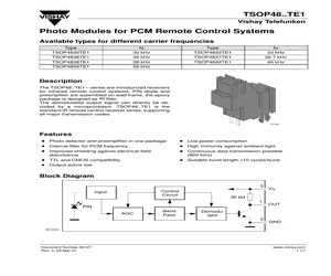
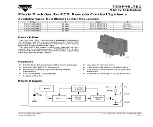
TSOP4838TE1 TSOP4856TE1 fo 30 kHz 36 kHz 38 kHz 56 kHz Type TSOP4833TE1 TSOP4837TE1 TSOP4840TE1 fo 33 kHz 36.7 kHz 40 kHz Description The TSOP48..TE1 - series are miniaturized receivers for infrared remote control systems. PIN diode and preamplifier are assembled on lead frame, the epoxy package is designed as IR filter. The demodulated output signal can directly be decoded by a microprocessor. TSOP48..TE1 is the standard IR remote control receiver series, supporting all major transmission codes. 16 080 Features D Photo detector and preamplifier in one package D Internal filter for PCM frequency D Improved shielding against electrical field D Low power consumption D High immunity against ambient light D Continuous data transmission possible (800 bit/s) disturbance D Suitable burst length 10 cycles/burst D TTL and CMOS compatibility D Output active low Block Diagram 3 Control Circuit Input 30 kW 1 PIN AGC Band Pass VS OUT Demodulator 2 GND 9612226 Document Number 82127 Rev. 3, 29-Mar-01 www.vishay
 7 Pages, 149 KB, Original
TSOP4838TE1 TSOP4856TE1 fo 30 kHz 36 kHz 38 kHz 56 kHz Type TSOP4833TE1 TSOP4837TE1 TSOP4840TE1 fo 33 kHz 36.7 kHz 40 kHz Description The TSOP48..TE1 - series are miniaturized receivers for infrared remote control systems. PIN diode and preamplifier are assembled on lead frame, the epoxy package is designed as IR filter. The demodulated output signal can directly be decoded by a microprocessor. TSOP48..TE1 is the standard IR remote control receiver series, supporting all major transmission codes. 16 080 Features D Photo detector and preamplifier in one package D Internal filter for PCM frequency D Improved shielding against electrical field D Low power consumption D High immunity against ambient light D Continuous data transmission possible (800 bit/s) disturbance D Suitable burst length 10 cycles/burst D TTL and CMOS compatibility D Output active low Block Diagram 3 Control Circuit Input 30 kW 1 PIN AGC Band Pass VS OUT Demodulator 2 GND 9612226 Document Number 82127 Rev. 1, 26-Apr-00 www.vishay
 7 Pages, 107 KB, Original
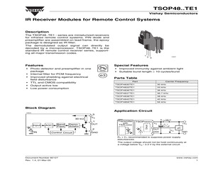
compatibility * Output active low * Low power consumption * Improved immunity against ambient light * Suitable burst length 10 cycles/burst e3 Parts Table Part Carrier Frequency TSOP4830TE1 30 kHz TSOP4833TE1 33 kHz TSOP4836TE1 36 kHz TSOP4837TE1 36.7 kHz TSOP4838TE1 38 kHz TSOP4840TE1 40 kHz TSOP4856TE1 56 kHz Block Diagram Application Circuit 16833 3 16842 1 Input AGC Band Pass Demodulator OUT 2 PIN Control Circuit GND Transmitter TSOPxxxx with TSALxxxx Circuit 30 k VS R1 = 100 VS OUT GND +VS C1 = 4.7 F C VO GND R1 + C1 recommended to suppress power supply disturbances. The output voltage should not be hold continuously at a voltage below VO = 3.3 V by the external circuit. Document Number 82127 Rev. 1.4, 01-Mar-05 www.vishay.com 1 TSOP48..TE1 Vishay Semiconductors Absolute Maximum Ratings Absolute Maximum Ratings Tamb = 25 C, unless otherwise specified Symbol Value Supply Voltage Parameter (Pin 2) Test condition VS - 0.3 to + 6.0 V Supply Current (Pin 2) IS 5 mA Output Voltage (Pin 1) VO - 0.3
 7 Pages, 234 KB, Original
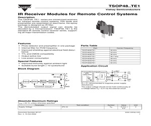
compatibility * Output active low * Low power consumption * Improved immunity against ambient light * Suitable burst length 10 cycles/burst e3 Parts Table Part Carrier Frequency TSOP4830TE1 30 kHz TSOP4833TE1 33 kHz TSOP4836TE1 36 kHz TSOP4837TE1 36.7 kHz TSOP4838TE1 38 kHz TSOP4840TE1 40 kHz TSOP4856TE1 56 kHz Block Diagram Application Circuit 16833 3 16842 1 Input AGC Band Pass Demodulator OUT 2 PIN Control Circuit GND Transmitter TSOPxxxx with TSALxxxx Circuit 30 k VS R1 = 100 VS OUT GND +VS C1 = 4.7 F C VO GND R1 + C1 recommended to suppress power supply disturbances. The output voltage should not be hold continuously at a voltage below VO = 3.3 V by the external circuit. Document Number 82127 Rev. 1.4, 01-Mar-05 www.vishay.com 1 TSOP48..TE1 Vishay Semiconductors Absolute Maximum Ratings Absolute Maximum Ratings Tamb = 25 C, unless otherwise specified Symbol Value Supply Voltage Parameter (Pin 2) Test condition VS - 0.3 to + 6.0 V Supply Current (Pin 2) IS 5 mA Output Voltage (Pin 1) VO - 0.3
 8 Pages, 261 KB, Original
* Output active low * Low power consumption Special Features * Improved immunity against ambient light * Suitable burst length 10 cycles/burst Parts Table Part Carrier Frequency TSOP4830TE1 30 kHz TSOP4833TE1 33 kHz TSOP4836TE1 36 kHz TSOP4837TE1 36.7 kHz TSOP4838TE1 38 kHz TSOP4840TE1 40 kHz TSOP4856TE1 56 kHz Application Circuit Block Diagram 30 k Circuit 3 Transmitter TSOPxxxx with TSALxxxx VS 1 Input AGC Band Pass Demodulator Control Circuit VS +VS C1 = 4.7 F OUT GND C VO GND OUT 2 PIN R1 = 100 GND R1 + C1 recommended to suppress power supply disturbances. The output voltage should not be hold continuously at a voltage below VO = 3.3 V by the external circuit. Absolute Maximum Ratings Tamb = 25 C, unless otherwise specified Parameter Supply Voltage Document Number 82127 Rev. 4, 15-Oct-2002 Test condition (Pin 2) Symbol Value Unit VS - 0.3 to + 6.0 V www.vishay.com 1 TSOP48..TE1 VISHAY Vishay Semiconductors Symbol Value Unit Supply Current Parameter (Pin 2) Test condition IS 5 mA Output Voltag
 7 Pages, 212 KB, Original


