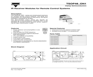
compatibility * Output active low * Low power consumption * Improved immunity against ambient light * Suitable burst length 10 cycles/burst e3 Parts Table Part Carrier Frequency TSOP4830ON1 30 kHz TSOP4833ON1 33 kHz TSOP4836ON1 36 kHz TSOP4837ON1 36.7 kHz TSOP4838ON1 38 kHz TSOP4840ON1 40 kHz TSOP4856ON1 56 kHz Block Diagram Application Circuit 16833 3 16842 1 Input AGC Band Pass Demodulator OUT 2 PIN Control Circuit GND Transmitter TSOPxxxx with TSALxxxx Circuit 30 k VS R1 = 100 VS OUT GND +VS C1 = 4.7 F C VO GND R1 + C1 recommended to suppress power supply disturbances. The output voltage should not be hold continuously at a voltage below VO = 3.3 V by the external circuit. Document Number 82088 Rev. 1.6, 01-Mar-05 www.vishay.com 1 TSOP48..ON1 Vishay Semiconductors Absolute Maximum Ratings Absolute Maximum Ratings Tamb = 25 C, unless otherwise specified Symbol Value Supply Voltage Parameter (Pin 2) Test condition VS - 0.3 to + 6.0 V Supply Current (Pin 2) IS 5 mA Output Voltage (Pin 1) VO - 0.3
 8 Pages, 604 KB, Original
mponent in accordance to RoHS 2002/95/EC and WEEE 2002/96/EC * Improved immunity against ambient light * Suitable burst length 10 cycles/burst Parts Table Part Carrier Frequency TSOP4830ON1 30 kHz TSOP4833ON1 33 kHz TSOP4836ON1 36 kHz TSOP4837ON1 36.7 kHz TSOP4838ON1 38 kHz TSOP4840ON1 40 kHz TSOP4856ON1 56 kHz Block Diagram Application Circuit 16842 3 30 k VS 1 Input AGC Band Pass Demodulator OUT 2 PIN Control Circuit GND Transmitter TSOPxxxx with TSALxxxx Circuit 16833 R1 = 100 VS OUT GND + VS C1 = 4.7 F C VO GND R1 and C1 recommended to suppress power supply disturbances. The output voltage should not be hold continuously a a voltage below VO = 3.3 V by the external circuit. Document Number 82088 Rev. 1.6, 01-Mar-05 www.vishay.com 1 TSOP48..ON1 Vishay Semiconductors Absolute Maximum Ratings Absolute Maximum Ratings Tamb = 25 C, unless otherwise specified Symbol Value Supply Voltage Parameter (Pin 2) Test condition VS - 0.3 to + 6.0 V Supply Current (Pin 2) IS 5 mA Output Voltage (Pin 1) VO - 0
 8 Pages, 564 KB, Original
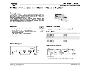
mponent in accordance to RoHS 2002/95/EC and WEEE 2002/96/EC * Improved immunity against ambient light * Suitable burst length 10 cycles/burst Parts Table Part Carrier Frequency TSOP4830ON1 30 kHz TSOP4833ON1 33 kHz TSOP4836ON1 36 kHz TSOP4837ON1 36.7 kHz TSOP4838ON1 38 kHz TSOP4840ON1 40 kHz TSOP4856ON1 56 kHz Block Diagram Application Circuit 16842 3 30 k VS 1 Input AGC Band Pass Demodulator OUT 2 PIN Control Circuit GND Transmitter TSOPxxxx with TSALxxxx Circuit 16833 R1 = 100 VS OUT GND + VS C1 = 4.7 F C VO GND R1 and C1 recommended to suppress power supply disturbances. The output voltage should not be hold continuously a a voltage below VO = 3.3 V by the external circuit. Document Number 82088 Rev. 1.6, 01-Mar-05 www.vishay.com 1 TSOP48..ON1 Vishay Semiconductors Absolute Maximum Ratings Absolute Maximum Ratings Tamb = 25 C, unless otherwise specified Symbol Value Supply Voltage Parameter (Pin 2) Test condition VS - 0.3 to + 6.0 V Supply Current (Pin 2) IS 5 mA Output Voltage (Pin 1) VO - 0
 7 Pages, 534 KB, Original
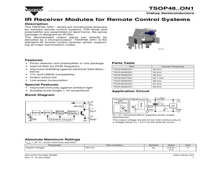
* Output active low * Low power consumption Special Features * Improved immunity against ambient light * Suitable burst length 10 cycles/burst Parts Table Part Carrier Frequency TSOP4830ON1 30 kHz TSOP4833ON1 33 kHz TSOP4836ON1 36 kHz TSOP4837ON1 36.7 kHz TSOP4838ON1 38 kHz TSOP4840ON1 40 kHz TSOP4856ON1 56 kHz Application Circuit Block Diagram 30 k Circuit 3 Transmitter TSOPxxxx with TSALxxxx VS 1 Input AGC Band Pass Demodulator Control Circuit VS +VS C1 = 4.7 F OUT GND C VO GND OUT 2 PIN R1 = 100 GND R1 + C1 recommended to suppress power supply disturbances. The output voltage should not be hold continuously at a voltage below VO = 3.3 V by the external circuit. Absolute Maximum Ratings Tamb = 25 C, unless otherwise specified Parameter Supply Voltage Document Number 82088 Rev. 6, 15-Oct-2002 Test condition (Pin 2) Symbol Value Unit VS - 0.3 to + 6.0 V www.vishay.com 1 TSOP48..ON1 VISHAY Vishay Semiconductors Symbol Value Unit Supply Current Parameter (Pin 2) Test condition IS 5 mA Output Voltag
 7 Pages, 297 KB, Original
-CV-003 E/P WITH S/W STEREO(068B) D3.5 ACCESSORIES A1 3828VA0474A MANUAL,OWNERS EN 090A/D TX A2 6710V00124D REMOTE CONTROLLER, MC049B W/O TXT MISCELLANEOUS F1111 0FS4001B53C FUSE,SLOW BLOW 4000MA 250 V 5.2X20 PA1101 6726VV0006D REMOTE CONTROLLER RECEIVER, TSOP4838ON1 SK901 6620VBC003A SOCKET (CIRC),CPT PCS030A 8PIN - 26 - DESCRIPTION FBT, BSC25-N1648 21 YY . VARISTOR, TVR621D14A THINKING 620V 10% P/NO: 3854VA0162A - S1 2004.6.12 SVC. SHEET : 3854VA0162A-S P/NO : 3828VD0196V Sep.,2004 Printed in Korea
 29 Pages, 3496 KB, Original
compatibility * Output active low * Low power consumption * Improved immunity against ambient light * Suitable burst length 10 cycles/burst e3 Parts Table Part Carrier Frequency TSOP4830ON1 30 kHz TSOP4833ON1 33 kHz TSOP4836ON1 36 kHz TSOP4837ON1 36.7 kHz TSOP4838ON1 38 kHz TSOP4840ON1 40 kHz TSOP4856ON1 56 kHz Block Diagram Application Circuit 16833 3 16842 1 Input AGC Band Pass Demodulator OUT 2 PIN Control Circuit GND Transmitter TSOPxxxx with TSALxxxx Circuit 30 k VS R1 = 100 VS OUT GND +VS C1 = 4.7 F C VO GND R1 + C1 recommended to suppress power supply disturbances. The output voltage should not be hold continuously at a voltage below VO = 3.3 V by the external circuit. Document Number 82088 Rev. 1.6, 01-Mar-05 www.vishay.com 1 TSOP48..ON1 Vishay Semiconductors Absolute Maximum Ratings Absolute Maximum Ratings Tamb = 25 C, unless otherwise specified Symbol Value Supply Voltage Parameter (Pin 2) Test condition VS - 0.3 to + 6.0 V Supply Current (Pin 2) IS 5 mA Output Voltage (Pin 1) VO - 0.3
 7 Pages, 603 KB, Original
 0RD4701F609 4.7K OHM 1/6 W 5% TA52 R90 0RD1000F609 100 OHM 1/6 W 5% TA52 R901 0RD2200F609 220 OHM 1/6 W 5.00% TA52 F801 0FS4001B53C FUSE,SLOW BLOW 4000MA 250 V 5.2X20 R902 0RD2200F609 220 OHM 1/6 W 5.00% TA52 PA1101 6726VV0006D REMOTE CONTROLLER RECEIVER,TSOP4838ON1 R903 0RD2200F609 220 OHM 1/6 W 5.00% TA52 SK901 6620VBC003A SOCKET (CIRC),CPT PCS030A 8PIN 14/360 R904 0RD4700F609 470 OHM 1/6 W 0.05 TA52 T402 6174V-5003A FBT,BSC28-N2325 29 YINYANG 6003LB+115V VE R905 0RD7501F609 7.5K OHM 1/6 W 5.00% TA52 TH801 163-058D THERMISTOR,PTC 03-07MX JA HWA 7 OHM 20% R906 0RD1000F609 100 OHM 1/6 W 5% TA52 TU101 6700MF0001E TUNER,TAFD-Z242D LG MULTI FS 4SYS,DIN R907 0RD1000F609 100 OHM 1/6 W 5% TA52 VD801 164-003K R908 0RD1000F609 100 OHM 1/6 W 5% TA52 R909 0RCZVTA002D 1/2 W 1.5K,10%,PLIKOR(HIGH SURGE) R910 0RCZVTA002D 1/2 W 1.5K,10%,PLIKOR(HIGH SURGE) R911 0RCZVTA002D 1/2 W 1.5K,10%,PLIKOR(HIGH SURGE) R912 0RD2204H609 2.2M OHM 1/2 W 5.00% TA52 SWITCH RWR 15W 1.0 OHM J PD SDKEA3 ALPS IEC 250V 8A HORIZONTAL
 32 Pages, 5811 KB, Original


