LM317H LM324J LM324N LM337K LM337K LM337T LM340K-5.0 LM340K-8.0 LM340K-12 LM340K-24 LM350K MC1455P1 MC3456P MC3556L PIC600 SG613 CR02AM-8 MC1723CL MC1723CP MC1723CG MC1723L MC1723G MC1733CP MC1733CG MC1733L MC1733G MC1741CP1 MC1741CG MC1741SCP1 MC1741SCG MC1741SG MC1741G MC1747CL MC1747CP2 MC1747CG MC1747L MC1747G MC1748CG MC1748G MC1436CG MC1436U MC1436G MC1456CG MC1456G MC1458P1 MC1458G MC1468L MC1495L MC1496L MC1496G MC1568L MC1568G MC1503U UA337KC SG1524C BEA SG1536T SG1556T SG1558T SG1568J SG1568T SG1595D SG1596D SG1596T SG2501D SG2501T SG2525A SG3081N SG3082 SG3401N SG3501T SG3503 SG3503Y SG3524 SG3524CD SG3524J SG3524P SG3525A SG3527A SG4501D SG4501J LTC921 SG7805ACK SG7805ACP SG7805AK SG7805CP SG7805K SG7806ACP SG7806CK SG7806CP SG7806K SG7808ACP SG7808CK SG7808CP SG7808K SG7812ACK SG7812ACP SG7815ACK SG7815AK SG7815CK SG7815CP SG7815K SG7818ACK SG7818AK SG7818CK SG7818CP SG7818K SG7824ACP SG7824CK SG1524CF MC1536G MC1556G MC1558G MC1568L MC1568G MC1595L MC1596L MC1596G MC1468L MC1468G U
 314 Pages, 275 KB, Original
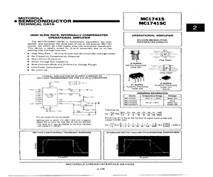
TRANSFORMATION FOR A D-TO-A CONVERTER a . voc =50V Vret 20 Va ' Al>R2 rox. D SUFFIX Roreeen P1 SUFFIX PLASTIC PACKAGE PLASTIC PACKAGE CASE 751 MSB AI [te CASE 626 {SO-8) A2 15, ORDERING INFORMATION a3 MC 15081 8 oh aa = Device Temperature Range Package AS MC1741SG -58C to + 126C Metal Can . MC1741SCD 80-8 * Vo MC1741SCG OC to +70C Metal Can LSB 48 MC1741SCP1 Plastic DIP 3 Theoretical Vg Veg=15 2 Veet ig ) AT A2 AS A4 AB AG A? AB Of [2 ae 1632 ea 128 286 Pins not shown are not connected. Adjust Vref, Al or RQ so that Vg with ali digital inputs at high level Settling time to within 1/2 LSB (19.5 mV) ts approxr is equal to 9.961 vaits. mately 4.0 us from the time that all bits are switched. "The value of C may be selected to minimize overshoot 2v Vitti iid | I 255 u Vo =~-(5k) [zt -+-+ + + + _+__|=10V J| =9.961V and ringing (C ~ 150 pF}. 1k 294 8 16 92 64 128 256 256 MC1741S LARGE-SIGNAL TRANSIENT RESPONSE STANDARD MC1741 versus MC1741S RESPONSE COMPARISON > >| Q a > >| a a a 3 1.0 us/DIV 10 ps/DIV
 6 Pages, 158 KB, Scan
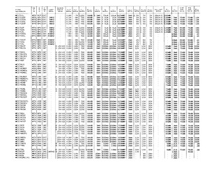
 IN| |N IT JE- JE+ yV- JN) JN JT! R [V+ [NIN JN 741MHS00 = [0 JMC1741SCP DIL-8/1P |T |E- JE+ |V- |T* |+ JN IN T41CHSPA 0 }MC1741SCP1 DIL-8/1C |T |E- JE+ |V- |T* |+ [NIN T41CHSPA |0. |MC.1741SCU TOS-8/1M |T JE- {E+ |-M|T* JR |+ [N foe ted. fed. 741MHSTY 0 {MC1741SG DIL-14/1C IN IN JT |E- JE+ |V- JN) IN JT* ]R |+ JN IN IN 741MHS0D = (0. {MC1741SL DIL-8/1C |T |E- JE+ |V- |T* |+ IN IN . 0. 1MC1741SU DIL-8/1C jT |E- [E+ |V- |T* |V+ JN IN foe ped. fed. : (0 (MC 1741U FLP-14/3C |E-1/E+1|T1 |V- |T2 |E+2|E-2 |T*2\+2,R2 |N {R1 W+l/T*d . LM747CF (0 |MC1747CF TOS-10/1M RL |V+1JE-1]E+1|V- jE+2 }E-2 |V+2 jR2 |N ef. de]. TBBO747 UA747HC = (0. 1MC.1747CG DIL-14/1C jE-L/E+1|T1 |V- [72 |E+2 |E-2 (T*2 |+21R2 IN {RL f+1)T*d TBBO747A = |UA7470C 10 MC1747CL DIL-14/1P JE-1/E+1|T1 |V- |T2 JE+2)E-217*2(V+21R2 |N {RL f+l/T*4 TBBO747A = |UA7470C 0 {MC1747CP FLP-14/3C 1E-L/E+1|T1 |- |T2 JE+2|E-2 |T*2|V+21R2 |N [R1 f+i/T*] . LM747F 10 |MC1747F TOS-10/1M IRL |V+1|E-1JE+1|V- |E+2 }E-2 |+2 (R2 | N fe ded. SFC2747M = |UA747HM 0
 12 Pages, 520 KB, Scan
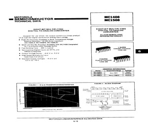
NT TO VOLTAGE CONVERSION Vref = 2.0 Vde R14 = R16 = 1.0 kO Ro = 5.0k0 Theoretical Vo MSB A1o=1 Vret Vo = Hef (Ro) [# + A2 AS, Adjust Vref, R14 or Ro so that Vo with all digital inputs at high level is equal to 9.961 volts. Vo = = (5k) Vo = 10V [=| = 9961V MC1741SG 16 or Equiv. VEE pF -20 Al A2. AS, A4 AS AB OA? A8 stato ++ 2 4 8 16 32 64 128 256 MOTOROLA LINEAR/INTERFACE ICs DEVICE DATA 6-22MC1408, MC1508 APPLICATIONS INFORMATION (continued) Voltage outputs of a larger magnitude are obtainable with this circuit which uses an external operational amplifier as a current to voltage converter. This configuration automatically keeps the output of the MC1408 at ground potential and the operational amplifier can generate a positive voltage limited only by its positive supply voltage. Frequency response and settling time are primarily determined by the characteristics of the operational amplifier. In addition, the operational amplifier must be compensated for unity gain, and in some cases overcompensatio
 12 Pages, 674 KB, Scan


