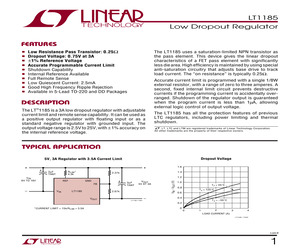
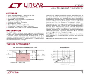
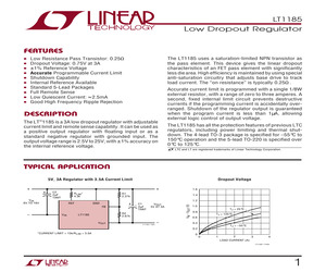
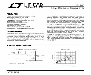
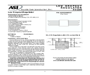
oltage .............................................................. 7V Output Voltage ........................................................ 30V Output Reverse Voltage ............................................ 2V Operating Ambient Temperature Range LT1185C ............................................... 0C to 70C LT1185M ......................................... - 55C to 125C Operating Junction Temperature Range* Control Section LT1185C ............................................. 0C to 125C LT1185I .......................................... - 40C to 125C LT1185M ........................................ - 55C to 150C Power Transistor Section LT1185C ............................................. 0C to 150C LT1185I .......................................... - 40C to 150C LT1185M ........................................ - 55C to 175C Storage Temperature Range ................ - 65C to 150C Lead Temperature (Soldering, 10 sec)................ 300C BOTTOM VIEW GND ORD
 16 Pages, 230 KB, Original
oltage .............................................................. 7V Output Voltage ........................................................ 30V Output Reverse Voltage ............................................ 2V Operating Ambient Temperature Range LT1185C ............................................... 0C to 70C LT1185I ............................................. - 40C to 85C LT1185M (OBSOLETE) .................... - 55C to 125C *See Application Section for details on calculating Operation Junction Temperature Operating Junction Temperature Range* Control Section LT1185C ............................................. 0C to 125C LT1185I .......................................... - 40C to 125C LT1185M (OBSOLETE) ................... - 55C to 150C Power Transistor Section LT1185C ............................................. 0C to 150C LT1185I .......................................... - 40C to 150C LT1185M (OBSOLETE) ................... - 55C to 175C Storage Temper
 16 Pages, 180 KB, Original
oltage .............................................................. 7V Output Voltage ........................................................ 30V Output Reverse Voltage ............................................ 2V Operating Ambient Temperature Range LT1185C ............................................... 0C to 70C LT1185M (OBSOLETE) .................... - 55C to 125C *See Application Section for details on calculating Operation Junction Temperature Operating Junction Temperature Range* Control Section LT1185C ............................................. 0C to 125C LT1185I .......................................... - 40C to 125C LT1185M (OBSOLETE) ................... - 55C to 150C Power Transistor Section LT1185C ............................................. 0C to 150C LT1185I .......................................... - 40C to 150C LT1185M (OBSOLETE) ................... - 55C to 175C Storage Temperature Range ................ - 65C to 150C Lead Temperature (Solder
 16 Pages, 220 KB, Original
oltage .............................................................. 7V Output Voltage ........................................................ 30V Output Reverse Voltage ............................................ 2V Operating Ambient Temperature Range LT1185C ............................................... 0C to 70C LT1185M ......................................... - 55C to 125C Operating Junction Temperature Range* Control Section LT1185C ............................................. 0C to 125C LT1185I .......................................... - 40C to 125C LT1185M ........................................ - 55C to 150C Power Transistor Section LT1185C ............................................. 0C to 150C LT1185I .......................................... - 40C to 150C LT1185M ........................................ - 55C to 175C Storage Temperature Range ................ - 65C to 150C Lead Temperature (Soldering, 10 sec)................ 300C BOTTOM VIEW GND ORD
 16 Pages, 215 KB, Original
imize heating. DC regulation will be affected by thermal regulation and temperature coefficient of the reference. See Application Section for details. Note 7: Guaranteed by design and correlation to other tests, but not tested. Note 8: Tjygin = 0C for the LT1185C, 40C for LT11851, and -55C for the LT1185M. Power transistor area and control circuit area have different maximum junction temperatures. Control area limits are T jax = 125C for the LT1185C and LT11851 and 150C for the LT1185M. Power area limits are 150C for LT1185C and LT1185! and 175C for LT1185M. Note 9: Vsat is the maximum specified dropout voltage; 0.25V + 0.25 x lout: Note 10: Current limit is programmed with a resistor from REF pin to GND pin. The value is 15k/I,\1y. Note 11: For Viy Vout = 1.5V; Vin = 5V, Vout = 3.5V. Vout = 1V for all other current limit tests. LY WhineLT1185 TYPICAL PERFORMANCE CHARACTERISTICS OUTPUT CURRNT (A) CURRENT (mA) Internal Current Limit TYPICAL @ TEST POINTS 0 5 10 15 20 25 3
 16 Pages, 618 KB, Scan
5CT-5-ND LT1176CN8-ND LT1176CN8-5-ND LT1176CSW-ND LT1176CSW-5-ND LT1178ACN8-ND LT1178CN8-ND LT1178SW-ND LT1178S8-ND LT1179ACN-ND LT1179CN-ND LT1179SW-ND LT1180ACN-ND LT1180ACSW-ND LT1181ACN-ND LT1181ACSW-ND LT1182CS-ND LT1183CS-ND LT1184CS-ND LT1184FCS-ND LT1185CT-ND LT1187CN8-ND LT1187CS8-ND LT1188CT-ND LT1189CN8-ND LT1189CS8-ND LT1191CN8-ND LT1191CS8-ND LT1193CN8-ND LT1195CN8-ND LT1195CS8-ND LT1203CN8-ND LT1203CS8-ND LT1204CN-ND LT1204CSW-ND LT1205CS-ND LT1206CS8-ND LT1208CN8-ND LT1208CS8-ND LT1209CN-ND LT1209CS-ND LT1211CN8-ND LT1211CS8-ND LT1212CN-ND LT1212CS-ND LT1213CN8-ND LT1213CS8-ND LT1214CN-ND LT1214CS-ND LT1215CN8-ND LT1215CS8-ND LT1216CN-ND LT1216CS-ND LT1218CN8-ND LT1218CS8-ND LT1218LCN8-ND LT1218LCS8-ND LT1219CN8-ND LT1219CS8-ND Data Book (Sold Sep.) Description Pkg. 9210B-ND 5V or 12V Supply RS232 4 Drivers/ 4 Receivers with Shut Down . . . . . . . . . . . . . . . . . . . SO-24 9210B-ND RS232 5 Drivers/3 Receivers w/Shut Down . . . . 24-Dip 9210B-ND RS232 5 Drivers/3 Receivers w/Sh
 531 Pages, 19076 KB, Original
SM TS host OP: NN COMP: 20-07-11 Hour: 09:52 TS:TS date TS time ANALOG, LOGIC & SENSOR ICS Find Datasheets Online LINEAR REGULATORS 1 LOW DROP OUT LINEAR REGULATORS (CONT.) LOW DROP OUT LINEAR REGULATORS (CONT.) Mfg. Part No. LT1175IS8#PBF LT1175IST-5#PBF LT1185CQ#PBF LTC1258CMS8#PBF LT3050EDDB-5#PBF LT3050EDDB-3.3#PBF LT3071MPUFD#PBF LT3071EUFD#PBF LT3050MPMSE-5#PBF LT3050MPMSE-3.3#PBF LT3050EMSE-5#PBF LT3050EMSE-3.3#PBF LT1461ACS8-2.5#PBF LT1461ACS8-4#PBF LT1461AIS8-5#PBF LT1461CCS8-4#PBF LT1461DHS8-2.5#PBF LT1461DHS8-3#PBF LT1461DHS8-5#PBF LT1521CS8#PBF LT1521CST-3.3#PBF LT1521CST-5#PBF LT1521IS8-3.3#PBF LT1521IS8-5#PBF LT1528CQ#PBF LT1529CQ-3.3#PBF LT1529CQ-5#PBF LT1529CQ#PBF LT1529CT#PBF LT1529IQ#PBF LT1585CM#PBF LT1585CM-3.3#PBF LT1585CT-3.3#PBF LT1587CM-3.3#PBF LT1761IS5-SD#PBF LT1761IS5-BYP#PBF LT1761IS5-5#PBF LT1761IS5-3.3#PBF LT1761IS5-3.0#PBF LT1761IS5-2.8#PBF LT1761IS5-2.5#PBF LT1761IS5-2.0#PBF LT1761IS5-1.8#PBF LT1761IS5-1.5#PBF LT1761IS5-1.2#PBF LT1762EMS8#PBF LT1762EMS8-2.5#PBF LT1
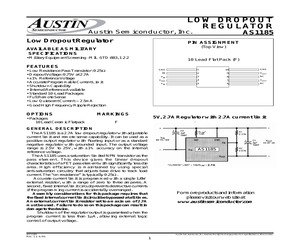
 375 Pages, 58008 KB, Original
teed by design and correlation to other tests, but not tested. 9. TJMIN = - 40C for AS1185I and -55C for the AS1185M. Power transistor area and control circuit area have different maximum junction temperatures. Control area limits are TJMAX = 125C for the LT1185C and LT1185I and 150C for the LT1185M. Power area limits are 150C for AS1185I and 175C for AS1185M. 10. VSAT is the maximum specified dropout voltage; 0.25V + 0.25 * IOUT. 11. Current limit is programmed with a resistor from REF pin to GND pin. The value is 15k/ILIM. 12. For VIN - VOUT = 1.5V; VIN = 5V, VOUT = 3.5V. VOUT = 1V for all other current limit tests. AS1185 Rev. 1.1 6/05 Austin Semiconductor, Inc. reserves the right to change products or specifications without notice. 2 LOW DROPOUT REGULA TOR REGULAT Austin Semiconductor, Inc. AS1185 ELECTRICAL CHARACTERISTICS: The * denotes specifications which apply over the operating temperature range, otherwise specifications are at TA = 25C. Adjustable version, VIN = 7.4V, VOUT = 5V, IOUT =
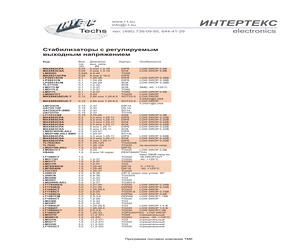
 7 Pages, 478 KB, Original
,3 1,25-11 3,3 1,25-11 5 1,25-11 5 1,25-11 1,23-57 1,23-37 3,3 1,25-11 3,3 1,25-11 5 1,25-11 1,25-125 1,25-125 1,23-37 5-20 5 16 . LT1086CT LM317AT LM317T LM317K LM78S40CN LM78S40N LT317AT L200CH L200C LM350K LM350T LM2596S-ADJ LT1764AEQ LT1764EQ LT1085CT LT1185CT LT1529CQ LT1587CM LT1084CT LM338K LM338T LT1084CP LT1084IT LT1585ACT LT1083CP LM337H LM2991S LM337K LM337T LM333K LT1033CT 1,5 1,5 1,5 1,5 1,5 1,5 1,5 2,0 2,0 3,0 3,0 3,0 3,0 3,0 3,0 3,0 3,0 3,0 5,0 5,0 5,0 5,0 5,0 5,0 7,5 0,5 1,0 1,5 1,5 3,0 3,0 1,2-37 1,2-37 1,2-37 1,25-40 1,25-40 1,25-37 2,8-36 2,8-36 1,2-33 1,2-33 1,2-37 1,21-20 1,21-20 1,25-28,5 2,5-25 3,8-14 2,5-3,6 1,2-29 1,2-32 1,2-32 1,25-28,5 1,25-28,5 2,5-3,6 1,25-33 -(1,2-37) -(2-25) -(1,2-37) -(1,2-37) -(1,2-32) -(1,2-32) DIP14 DIL14 SO14 TO100 SO8 LOW DROP 0,4 DIP8 LOW DROP 0,32 DIP8 LOW DROP 0,32 SO8 LOW DROP 0,32 SO8 LOW DROP 0,32 DIP8 LOW DROP 0,22 SO8 LOW DROP 0,22 DIP8 SO14L DIP8 LOW DROP 0,48 SO8 LOW DROP 0,32 DIP8 LOW DROP 0,32 TO220AB TO220 . DIP16 TO220 LOW DROP 0
 1 Pages, 40 KB, Original
teed by design and correlation to other tests, but not tested. 9. TJMIN = - 40C for AS1185I and -55C for the AS1185M. Power transistor area and control circuit area have different maximum junction temperatures. Control area limits are TJMAX = 125C for the LT1185C and LT1185I and 150C for the LT1185M. Power area limits are 150C for AS1185I and 175C for AS1185M. 10. VSAT is the maximum specified dropout voltage; 0.25V + 0.25 * IOUT. 11. Current limit is programmed with a resistor from REF pin to GND pin. The value is 15k/ILIM. 12. For VIN - VOUT = 1.5V; VIN = 5V, VOUT = 3.5V. VOUT = 1V for all other current limit tests. AS1185 Rev. 1.0 6/03 Austin Semiconductor, Inc. reserves the right to change products or specifications without notice. 2 LOW DROPOUT REGULA TOR REGULAT Austin Semiconductor, Inc. AS1185 ELECTRICAL CHARACTERISTICS: The * denotes specifications which apply over the operating temperature range, otherwise specifications are at TA = 25C. Adjustable version, VIN = 7.4V, VOUT = 5V, IOUT =
 7 Pages, 110 KB, Original
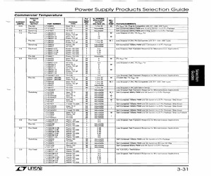
33 LT1085CK Steel TO-3 30 1.2 to 29 M, | | Low Dropout (1.2), Pin Compatible with 317, 350 Types LT1085CT T0-220 30 1.2 to 29 | Neg Adj LT1033CK Stee] TO-3 35 | -1.2 to-32 M | 2% Veer Tol LT1033CP Plastic TO-3P 35 | ~1.210-32 LT1033CT T0220 35 | ~1.2to-32 LT1185CT T0-220 35 ~2.5 to -25 M,1 | Low Dropout (0,75V) with Prog Current Limit and Shutdown Dual Pos LT1035CK Steel TO-3 20 | Two 5V Outputs | M | Logic Controtled Main Output Voltage, 75mA Auxillary Qutput Fixed LT1035CT T0-220 20 | Two SV Outputs Positive LT1036CK Steel 70-3 30 12,5 M | Logic Controtied 12V, 3A Output, 5V, 75mA Auxillary Output LT1036CT 70-220 30 12, Switching LT1371CR 7-Lead OD 30 Adjustable Self-Contained S00kH2z PWM and 3A Switch in a 7-Pin Package 25 Switching LT1071CK Steel TO-3 40 Adjustable M_ | Self-Contalned 40kHz PWM and 2.5A Switch in a 5-Pin Package LT1071CT 70-220 40 Adjustable I LT1071HVCK Stee! T0-3 60 Adjustable M LT1071HVCT T0-220 60 Adjustable | LT11710K Stee! T0-3 40 Adjustable M_ | Self-Contained 100kHz P
 5 Pages, 332 KB, Scan
33 LT1085CK Steel TO-3 30 1.2 to 29 M,| | Low Dropout (1.2V). Pin Compatible with 317, 350 Types LT1085CT 10-220 30 1.2 to 29 | Neg Adj LT1033CK Stee! TO-3 35 -1.2 to -32 M | 2% Vaee Tol LT1033CP Plastic TO-3P 35 ~1.2 to -32 LT1033CT T0-220 35 -1.2 to -32 LT1185CT 10-220 35 -2.5 to -25 M.1 | Low Dropout (0.75V) with Prag Current Limit and Shutdown Dual Pos LT1035CK Steel TO-3 20 | Two 5V Outputs M_ | Logic Controlled Main Output Voltage, 78mA Auxiliary Output Fixed LT1035CT [70-220 20 | Two 5V Outputs Positive LT1036CK Steel TO-3 30 12.5 M_ |Logic Controlled 12V, 3A Output, 5V, 75mA Auxiliary Output LT1036CT TO-220 30 12.5 Logic Controlied 12V, 3A Output, 5V, 75mA Auxiliary Qutput 25 Switching LT10710K Stee! TO-3 40 Adjustable M | Self-Contained 40kHz PWM and 2.5A Switch in a 5-Pin Package LT1071CT 10-220 40 Adjustable | LT1071HVCK Steel TO-3 60 Adjustable M LT1071HVCT T0-220 60 Adjustable | LT11710K Steel TO-3 40 Adjustable M {Self-Contained 100kHz PWM and 2.5A Switch in a 5-Pin Package LT4171CT
 1 Pages, 74 KB, Scan


