L JANTX2N3507AL 2N3507AL 182 30 X 182 30 JANTX2N1893 JANTX2N1893 2N1893 349 60 X 349 60 JANTXV2N3507AL JANTXV2N3507AL 182 30 X 182 30 JANTXV2N1893 JANTXV2N1893 349 60 X 349 60 JANS2N3507AL JANS2N3507AL 182 30 X X 391 182 30 JAN2N1893S JAN2N1893S 391 30 30 JAN2N3700 JAN2N3700 182 30 X X 391 182 30 JANTX2N1893S JANTX2N1893S 2N1893S JANTX2N3700 391 30 30 JANTX2N3700 182 182 JANTXV2N1893S JANTXV2N1893S 391 30 X 30 391 JANTXV2N3700 JANTXV2N3700 2N3700 270 20 270 20 391 30 X 30 391 JAN2N2060 JAN2N2060 JANS2N3700 JANS2N3700 391 30 30 270 20 X 391 270 20 JANSR2N3700 JANSR2N3700 JANTX2N2060 JANTX2N2060 2N2060 395 27 X 395 27 270 20 270 20 JAN2N3735 JAN2N3735 JANTXV2N2060 JANTXV2N2060 395 27 X X 395 27 JANTX2N3735JANTX2N3735 251 20 251 20 JAN2N2218 JAN2N2218 395 27 X 27 395 JANTXV2N3735 JANTXV2N3735 251 20 X 251 20 JANTX2N2218 JANTX2N2218 2N2218 2N3735 395 27 X 27 395 JANS2N3735 JANS2N3735 251 20 X 251 20 JANTXV2N2218 JANTXV2N2218 395 27 X 27 395 JANSR2N3735JAN2N2218A JANSR2N3735 251 20 X 251
 17 Pages, 6924 KB, Original
 of PINs. The following is a list of possible PINs available on this specification sheet. PINs for types 2N3019 (1) PINs for types 2N3019S (1) PINs for types 2N3057A (1) PINs for types 2N3700 (1) PINs for types 2N3700UB (1) JAN2N3019 JAN2N3019S JAN2N3057A JAN2N3700 JAN2N3700UB JANTX2N3019 JANTX2N3019S JANTX2N3057A JANTX2N3700 JANTX2N3700UB JANTXV2N3019 JANTXV2N3019S JANTXV2N3057A JANTXV2N3700 JANTXV2N3700UB JANS2N3019 JANS2N3019S JANS2N3057A JANS2N3700 JANS2N3700UB JANTXVR2N3019 JANTXVR2N3019S JANTXVR2N3057A JANTXVR2N3700 JANTXVR2N3700UB JANTXVF2N3019 JANTXVF2N3019S JANTXVF2N3057A JANTXVF2N3700 JANTXVF2N3700UB JANS#2N3019 JANS#2N3019S JANS#2N3057A JANS#2N3700 JANS#2N3700UB (1) The number sign (#) represents one of eight RHA designators available (M, D, P, L, R, F, G, or H). * 6.6.1 PINs for unencapsulated devices (die). The following is a list of possible PINs for unencapsulated devices available on this specification sheet. PINs for types 2N3019 (1) PINs for types 2N3700 (1) JANHCA2
 40 Pages, 1140 KB, Original
gs only. Functional operation above the Recommended Operating Conditions is not implied. Extended exposure to stresses above the Recommended Operating Conditions may affect device reliability. JANTX2N3019 JANTXV2N3019 JAN2N3019S JANTX2N3019S JANTXV2N3019S JAN2N3700 JANTX2N3700 JANTXV2N3700 (c) Semiconductor Components Industries, LLC, 2012 August, 2012 - Rev. 2 1 Publication Order Number: 2N3019/D 2N3019, 2N3019S, 2N3700 ELECTRICAL CHARACTERISTICS (TA = 25C unless otherwise noted) Symbol Characteristic Min Max Unit 80 - - - 10 10 nAdc mAdc - 10 nAdc - 10 mAdc 50 90 100 50 15 300 - 300 300 - - - 0.2 0.5 - 1.1 5.0 20 80 400 - 12 - 60 - 4.0 - 400 - 30 OFF CHARACTERISTICS V(BR)CEO Collector -Emitter Breakdown Voltage (IC = 30 mAdc) Emitter-Base Cutoff Current (VEB = 5.0 Vdc) (VEB = 7.0 Vdc) IEBO Collector-Emitter Cutoff Current (VCE = 90 Vdc) ICEO Collector-Base Cutoff Current (VCB = 140 Vdc) ICBO Vdc ON CHARACTERISTICS (Note 1) DC Current Gain (IC = 0.1 mAdc, VCE = 10 Vdc) (IC = 10 mAdc, VCE = 10 Vd
 5 Pages, 113 KB, Original
gs only. Functional operation above the Recommended Operating Conditions is not implied. Extended exposure to stresses above the Recommended Operating Conditions may affect device reliability. JANTX2N3019 JANTXV2N3019 JAN2N3019S JANTX2N3019S JANTXV2N3019S JAN2N3700 JANTX2N3700 JANTXV2N3700 (c) Semiconductor Components Industries, LLC, 2012 August, 2012 - Rev. 2 1 Publication Order Number: 2N3019/D 2N3019, 2N3019S, 2N3700 ELECTRICAL CHARACTERISTICS (TA = 25C unless otherwise noted) Symbol Characteristic Min Max Unit 80 - - - 10 10 nAdc mAdc - 10 nAdc - 10 mAdc 50 90 100 50 15 300 - 300 300 - - - 0.2 0.5 - 1.1 5.0 20 80 400 - 12 - 60 - 4.0 - 400 - 30 OFF CHARACTERISTICS V(BR)CEO Collector -Emitter Breakdown Voltage (IC = 30 mAdc) Emitter-Base Cutoff Current (VEB = 5.0 Vdc) (VEB = 7.0 Vdc) IEBO Collector-Emitter Cutoff Current (VCE = 90 Vdc) ICEO Collector-Base Cutoff Current (VCB = 140 Vdc) ICBO Vdc ON CHARACTERISTICS (Note 1) DC Current Gain (IC = 0.1 mAdc, VCE = 10 Vdc) (IC = 10 mAdc, VCE = 10 Vd
 8 Pages, 275 KB, Original
gs only. Functional operation above the Recommended Operating Conditions is not implied. Extended exposure to stresses above the Recommended Operating Conditions may affect device reliability. JANTX2N3019 JANTXV2N3019 JAN2N3019S JANTX2N3019S JANTXV2N3019S JAN2N3700 JANTX2N3700 JANTXV2N3700 (c) Semiconductor Components Industries, LLC, 2011 October, 2011 - Rev. 1 1 Publication Order Number: 2N3019/D 2N3019, 2N3019S, 2N3700 ELECTRICAL CHARACTERISTICS (TA = 25C unless otherwise noted) Characteristic Symbol Min Max Unit 80 - - - 10 10 nAdc mAdc - 10 nAdc - 10 mAdc 50 90 100 50 15 300 - 300 300 - - - 0.2 0.5 - 1.1 5.0 20 80 400 - 12 - 60 - 4.0 - 400 - 30 OFF CHARACTERISTICS Collector -Emitter Breakdown Voltage (IC = 30 mAdc) V(BR)CEO Emitter-Base Cutoff Current (VEB = 5.0 Vdc) (VEB = 7.0 Vdc) IEBO Collector-Emitter Cutoff Current (VCE = 90 Vdc) ICES Collector-Base Cutoff Current (VCB = 140 Vdc) ICBO Vdc ON CHARACTERISTICS (Note 1) DC Current Gain (IC = 0.1 mAdc, VCE = 10 Vdc) (IC = 10 mAdc, VCE = 10 V
 4 Pages, 101 KB, Original
gs only. Functional operation above the Recommended Operating Conditions is not implied. Extended exposure to stresses above the Recommended Operating Conditions may affect device reliability. JANTX2N3019 JANTXV2N3019 JAN2N3019S JANTX2N3019S JANTXV2N3019S JAN2N3700 JANTX2N3700 JANTXV2N3700 (c) Semiconductor Components Industries, LLC, 2012 August, 2012 - Rev. 2 1 Publication Order Number: 2N3019/D 2N3019, 2N3019S, 2N3700 ELECTRICAL CHARACTERISTICS (TA = 25C unless otherwise noted) Symbol Characteristic Min Max Unit 80 - - - 10 10 nAdc mAdc - 10 nAdc - 10 mAdc 50 90 100 50 15 300 - 300 300 - - - 0.2 0.5 - 1.1 5.0 20 80 400 - 12 - 60 - 4.0 - 400 - 30 OFF CHARACTERISTICS V(BR)CEO Collector -Emitter Breakdown Voltage (IC = 30 mAdc) Emitter-Base Cutoff Current (VEB = 5.0 Vdc) (VEB = 7.0 Vdc) IEBO Collector-Emitter Cutoff Current (VCE = 90 Vdc) ICEO Collector-Base Cutoff Current (VCB = 140 Vdc) ICBO Vdc ON CHARACTERISTICS (Note 1) DC Current Gain (IC = 0.1 mAdc, VCE = 10 Vdc) (IC = 10 mAdc, VCE = 10 Vd
 6 Pages, 113 KB, Original
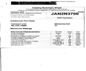
cument is a summary description of this device. Refer t to the detailed product datasheet or or manufacturing division for details. 9/22/98 _[Microsemi Corp. / Watertown Division 'Division Phone: (617)926-0404 Contact: Bob Stachowski i 4 nine ensiierortae JAN2N3700 NPN Transistor jeter { } } i i 3 1 Additional Part Data : Datasheet Link: MSC0279A.PDF MIL-PRF-19500: 391 Maximum Ratings _ Electrical Characteristic f Symbol Power Dissipation fr, Power Collector Current r CO ip : Breakdown Voltage Collector-to-Base a BVCBO a ols . Nolfage Collector to Emitter Open ~~ i Vceo _ Voltage Emitter to Bas Open Vbo HE Test Comaiiog mm e ARE Sie Tet ws P 155 : Collector Emitter Saturation Voltage } VCE(sat) _ MCE(sat) IC Test Condition [ VCEGaty @ IC VCE (eat) 1B Test Cori dition ne on ay 1S Q Bandwidth (min) ~ 4dil Sb | dl Sp --/6'9 | ---/0SZ 21 /-~~ | 090 /~~ /ge7L| ---/o009 Zo 1/1 Liv gro /8z0" EVI/PlL6 | 9ro' /9co zol'/--- | ogo /--- AL eL | Cd L OSO" G6b/2S 'a| S6L/8Z18 $3S/1Se | oz' /6028 Ser /90b's | 6
 2 Pages, 80 KB, Scan
n to average +3 and -3. Post-test distribution to average +4 and -4 of the pre-test results Pre-test distribution to average +3 and -3. Post-test distribution to average +4 and -4 of the pre-test results MIL-PRF-19500/694A Temperature-Power Derating Curve JAN2N3700UE1 Axial Leads 0.375" Mount (/585) Sinewave Operation Maximum Rating (%) 120 100 80 60 40 20 0 25 50 75 100 125 150 Leads 3/8" Temperature (C) Sinewave Operation 50% Duty Cycle Thermal Resistance Junction to Leads 3/8" = 560C/W 175 225 Note: Max Finish-Alloy Temp = 175.0C * FIGURE 2. Derating for 2N3700UE1 (SOT-23 similar to TO-236). 17 200 MIL-PRF-19500/694A NOTES: 1. The rise time (tr) of the applied pulse shall be 2.0 ns, duty cycle 2 percent and the generator source impedance shall be 50 ohms. 2. Sampling oscilloscope: ZIN 100 k, CIN 12 pF, rise time 2.0 ns. FIGURE 3. Nonsaturated switching-time test circuit. 18 MIL-PRF-19500/694A Note: Thickness: 1.5 mm (0.059 in) Copper leads: 0.3 mm (0.012 in) * FIGURE 4. Layout for RJA test. *
 21 Pages, 270 KB, Original
gs only. Functional operation above the Recommended Operating Conditions is not implied. Extended exposure to stresses above the Recommended Operating Conditions may affect device reliability. JANTX2N3019 JANTXV2N3019 JAN2N3019S JANTX2N3019S JANTXV2N3019S JAN2N3700 JANTX2N3700 JANTXV2N3700 (c) Semiconductor Components Industries, LLC, 2012 August, 2012 - Rev. 2 1 Publication Order Number: 2N3019/D 2N3019, 2N3019S, 2N3700 ELECTRICAL CHARACTERISTICS (TA = 25C unless otherwise noted) Symbol Characteristic Min Max Unit 80 - - - 10 10 nAdc mAdc - 10 nAdc - 10 mAdc 50 90 100 50 15 300 - 300 300 - - - 0.2 0.5 - 1.1 5.0 20 80 400 - 12 - 60 - 4.0 - 400 - 30 OFF CHARACTERISTICS V(BR)CEO Collector -Emitter Breakdown Voltage (IC = 30 mAdc) Emitter-Base Cutoff Current (VEB = 5.0 Vdc) (VEB = 7.0 Vdc) IEBO Collector-Emitter Cutoff Current (VCE = 90 Vdc) ICEO Collector-Base Cutoff Current (VCB = 140 Vdc) ICBO Vdc ON CHARACTERISTICS (Note 1) DC Current Gain (IC = 0.1 mAdc, VCE = 10 Vdc) (IC = 10 mAdc, VCE = 10 Vd
 4 Pages, 103 KB, Original
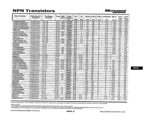
N2221A | Watertown | 10-18 STD | 255 | 19788/ 05 108 75 50 6 0.3 150 | 40 | 120 | | JANTXV2N2222A | Watertown | TO-18 STD| 255! 19791| 05 08: 75 ' 50/1 6 0.3 150 | 100 | 300 | | 2N3700 Watertown | TO-18 |STD 18696 05 | 1 | 140/ 80/7 | O2 150 | 100 | 300 _ JAN2N3700 Watertown ; TO-18 STD | 391 | 19899, 0.5 | 1 | 140 | 80 | 7 [| O2 150 100 300 | JANTX2N3700 Watertown | TO-18 STD_391 |19900| 0.5 | 1 | 140 80/7 | 02 150 | 100 ; 300 ; JANTXV2N3700__ Watertown | TO-18 STD_391 | 19901; 0.5 | 1 | 140! 80! 7 | ~O2 150 _ 100 | 300 2N3737 | Watertown TO-46 STD | [18697105 / 15175 40 5 0.5 500 40 | 140: , JAN2N3737 | Watertawn | TO-46 STD] 395/19909/ 05 115 75 4015 =) 05 500 | 40 | 140: _JANTX2N3737__| Watertown | TO-46 STD] 395 19910105 15 | 75 | 40) 5 | 05 500 40 | 140 | JANTXV2N3737_| Watertown | 10-46 {STD | 395 1991105 [15175 | 40, 5 | 05 500. 40 140. | 2NO696 Watertown | TO-5 STD | (19700 | 0.6 | 60 | 40 | 5; 15 150: 20 | 80 | 2N0697 Watertown | TO-5 STD 19703 | 0.6 (60! 40 5 | 15 150. 40 | 420 JAN2N06
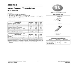
 1 Pages, 83 KB, Scan
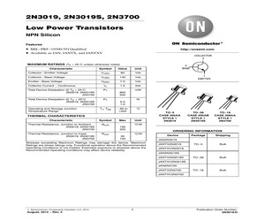
implied. Extended exposure to stresses above the Recommended Operating Conditions may affect device reliability. 1. This number assumes a substrate of 1 oz. thick copper and a copper area of 550 mm2. ORDERING INFORMATION Device Package Shipping TO-18 Bulk JAN2N3700 JANTX2N3700 JANTXV2N3700 (c) Semiconductor Components Industries, LLC, 2011 July, 2011 - Rev. 0 1 Publication Order Number: 2N3700/D 2N3700 ELECTRICAL CHARACTERISTICS (TA = 25C unless otherwise noted) Symbol Characteristic Min Max 50 90 100 50 15 300 - 300 300 - - - 0.2 0.5 - 1.1 - 12 5.0 20 Unit ON CHARACTERISTICS hFE DC Current Gain (IC = 0.1 mAdc, VCE = 10 Vdc) (Note 2) (IC = 10 mAdc, VCE = 10 Vdc) (Note 2) (IC = 150 mAdc, VCE = 10 Vdc) (Note 2) (IC = 500 mAdc, VCE = 10 Vdc) (Note 2) (IC = 1.0 Adc, VCE = 10 Vdc) (Note 2) Collector -Emitter Saturation Voltage (Note 2) (IC = 150 mAdc, IB = 15 mAdc) (IC = 500 mAdc, IB = 50 mAdc) VCE(sat) Base -Emitter Saturation Voltage (Note 2) (IC = 150 mAdc, IB = 15 mAdc) VBE(sat) - Vdc Vdc SMALL-SI
 3 Pages, 87 KB, Original


