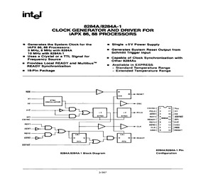
8284A-1 CLOCK GENERATOR AND DRIVER FOR iAPX 86, 88 PROCESSORS = Generates the System Clock for the = Single +5V Power Supply iAPX 86, 88 Processors: 5 MHz, 8 MHz with 8284A u Generates System Reset Output from 10 MHz with 8284A-1 Schmitt Trigger Input u Uses a Crystal or a TTL Signal for Frequency Source ' . T = Provides Local READY and Multibus = Available in EXPRESS READY Synchronization - Standard Temperature Range = 18-Pin Package - Extended Temperature Range = Capable of Clock Synchronization with Other 8284As RES > D Gt RESET XTAL OSCILLATOR x2 | p> ose _ csync(1 18 [ec FIC __-_1 PoLk C2 vox +3 +4 +2 pe PCLK | AENI(] 3 16 |_] x2 EFI SYNC SYNC ADVICE KSYNC CSYNC | reapy (15 14 EFI RDy2(] 6 CFIC ROY) KENG (]7 12[lose t > + | > cik __ ___ cLKCs 14 REN Cc RES GNDL]9 10 |) RESET ADY2 l CKt CKt REN? D Q D Qt READY FFA FF2 ASYNG 8284A/8284A-1 Pin 8284A/8284A-1 Block Diagram Configuration 3-5678284A/8284A-1 Table 1. Pin Description HIGH, CLK is ge
 8 Pages, 215 KB, Scan
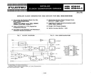
8284A-1 MBL 8284A April 1986 Edition 4.0 BIPOLAR CLOCK GENERATOR AND DRIVER FOR MBL 8086/8088/8089 Generates the System Clock for the @ Generates System Reset Output from MBL 8086/8088/8089 Schmitt Trigger Input Processors: . 5MHz and 8MHz with MBL 8284A @ Capable of Clock Synchronization with 10MHz with MBL 8284A-1 Other MBL 8284As Uses a Crystal or a TTL Signal for Single +5V Power Supply Frequency Source / @ 18-Pin Cerdip (Suffix: -CZ) Provides Local READY and Multibus* READY Synchronization Fig.1 BLOCK DIAGRAM Fig. 2 PIN CONFIGURATION AES NS RES Z, D bt QO} RESET {CK i x1 OSCILLATOR x2 | [>ore csync(1 187 Vee FIC PCLK(]2 170 x1 73 Fy fy] 72) poe PCLK AENIC}3 16[9x2 SYNC SYNC ROY1(}4 MBL 1517) ASYNC EFI csYNe ] J READYO 14D EF RDY2(16 13D F/E RDY1 AEN2C]7 120) osc _ t_f>>- cikC]s 11 RES AEN] eno 10) RESET I 1 RDY2 [ CK CKi AEN2 0 Qa D LHe READY FFA FF2 ASYNC: *Trade Mark of Intel Corporation Portions Reprinted by permission of Intel Corporation Intel Corporation, 1983 1-300AON FUJ
 11 Pages, 504 KB, Scan
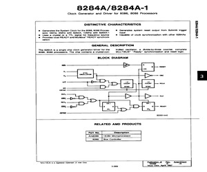
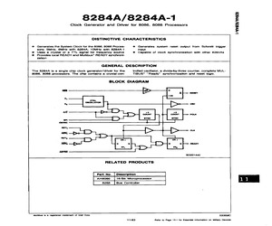
8284A-1 Clock Generator and Driver for 8086, 8088 Processors DISTINCTIVE CHARACTERISTICS @ Generates the System Clock for the 8086, 8088 Proces- @ Generates system reset output from Schmitt trigger sors: 5MHz, 8MHz with 8284A; 10MHz with 8284A-1 input @ Uses a crystal or a TTL signal for frequency source Capable of clock synchronization with other 8284As @ Provides local READY and Multibus* READY synchroni- zation GENERAL DESCRIPTION The 82844 is a single chip clock generator/driver for the trolled oscillator, a divide-by-three counter, complete 8086, 8088 processors. The chip contains a crystal-con- MULTIBUS* "Ready" synchronization and reset logic. BLOCK DIAGRAM RES [>_/> _ Qf RESET L-W8Z8/VPszcs maqick xy XTAL %;$~J osciiarorn [7] > osc Ae +3 +2 COUNT fb @| COUNT f pcLK fr SYNC SYNC sync _| RADY, t + >- cLK ER, ROY, l cKY cK} KEN, D a D @;-~ READY FF, FF2 ASYRC BD001440 RELATED AMD PRODUCTS Part No. Description Ams086 | 16-Bit Microprocessor 8288 | Bus Controller *MULTIBUS is a re
 10 Pages, 459 KB, Scan
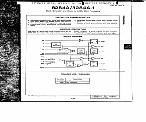
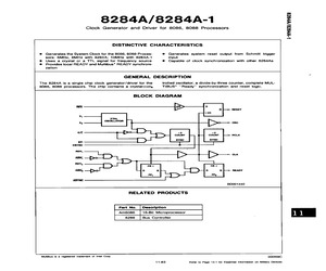
8284A-1 Clock Generator and Driver for 8086, 8088 Processors 8 DISTINCTIVE CHARACTERISTICS i @ Generates the System Clock for the 8086, 8088 Proces- @ Generates system reset output from Schmitt trigger sors: 5MHz, 8MHz with 8284A; 10MHz with 8284A-1 input ge @ Uses a crystal or a TTL signal for frequency source @ Capable of clock synchronization with other 8284As > @ Provides focal READY and Multibus* READY synchroni- oe zation GENERAL DESCRIPTION The 8284A is a single chip clock generator/driver for the trolled oscillator, a divide-by-three counter, complete 8086, 8088 processors. The chip contains a crystal-con- MULTIBUS* "Ready" synchronization and reset logic. BLOCK DIAGRAM RES > D @|- reser rick % XTAL Xe oscittaton, [7] y ose r/c +3 +2 COUNT J @{ COUNT [ PcLK en SYNC SYNC sync 4 J RDY, t_>>-++->> CLK AER; . RDY, I ; [ CKE cK) AER, D a D Q}~ READY FF, FFa ASYRG BD001440 RELATED AMD PRODUCTS Part No. Description Am8086 | 16-Bit Microprocessor 6288 | Bus Controller MULTIBUS fs a r
 10 Pages, 1108 KB, Scan
088/8089 @ Generates the System Clock for the @ Generates System Reset Output from MBL 8086/8088/8089 Schmitt Trigger Input Processors: Capable of Clock Synchronization with 5MHz and 8MHz with MBL 8284A @ Capable of Clock synchronization wi 10MHz with MBL 8284A-1 Other MBL 8284As Uses a Crystal or a TTL Signal for @ Single +5V Power Supply Frequency Source 18-Pin Cerdip (Suffix: -CZ) @ Provides Local READY and Multibus* READY Synchronization Fig.1 BLOCK DIAGRAM Fig. 2 PIN CONFIGURATION ~ RES TT D L G} RESET cKi x1 OSCILLATOR x2 | > osc csYNcC1 180 Vee F/C-_4 PCLK]2 1700x1 300 Ty 2 Pe PCLK AENICN3 jet x2 EFI sYNC_ f as Rovif|4 MBL 15(7 ASYNC csyne | READYCIS 14 er RDY2C16 13D F/C ROY1I AEN2 (7 127.) 0s _ pe cLKC}8 v1) RES AEN! cnoo 10 RESET RDY2 CKt Kt | AEN? D a |= READY FFI FF2 ASYNG *Trade Mark of Intel Corporation Portions Reprinted by permission of Intel Corporation Intel Corporation, 1983 4 AnnFUJITSU MICROELECTRONICS 97 DE) 37497b2 oOO4aNA 3 i PUNE | T-49-17-07 FUJITSU MBL 8284A HET MBL 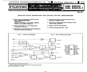 11 Pages, 326 KB, Scan
11 Pages, 326 KB, Scan8284A-1 Clock Generator and Driver for 8086, 8088 Processors DISTINCTIVE CHARACTERISTICS @ Generates the System Clock for the 8086, 8088 Proces- @ Generates system reset output from Schmitt trigger sors: 5MHz, 8MHz with 8284A; 10MHz with 8284A-1 input @ Uses a crystal or a TTL signal for frequency source @ Capable of clock synchronization with other 8284As @ Provides local READY and Multibus* READY synchroni- zation GENERAL DESCRIPTION The 8284A is a single chip clock generator/driver tor the trolled oscillator, a divide-by-three counter, complete MUL- 8086, 8088 processors. The chip contains a crystal-con- TIBUS* "Ready" synchronization and reset logic. BLOCK DIAGRAM - PPL we rapt cK x, XTAL Xe ron 1} > osc ee +a +2 court L., 24 count L~ ecix fA SYNC SYNC svnc 4 RDY, , -D>+-D>-+ KEN, nov, | CKt cal a, o a Q }-> READY FF, FRy Aavne BD001440 RELATED PRODUCTS Part No. | Description Am8086 | 16-Bit Microprocessor 8288 | Bus Controlier Multibus is a registered trademark of intel Corp. 03
 9 Pages, 229 KB, Scan
8284A-1 Clock Generator and Driver for 8086, 8088 Processors DISTINCTIVE CHARACTERISTICS @ Generates the System Clock for the 8086, 8088 Proces- @ Generates system reset output from Schmitt trigger sors: 5MHz, 8MHz with 8284A; 10MHz with 8284A-1 input . @ Uses a crystal or a TTL signal for frequency source @ Capable of clock synchronization with other 8284As Provides local READY and Multibus* READY synchroni- zation GENERAL DESCRIPTION The 8284A is a single chip clock generator/driver for the trolled oscillator, a divide-by-three counter, complete MUL- 8086, 8088 processors. The chip contains a crystal-cong TIBUS* ''Ready" synchronization and reset logic. BLOCK DIAGRAM RES > D ~~ G]- RESET q+cK XTAL Xe Tor [7] > ose ne +3 +2 count b @-{ COUNT }= PCLK SYNC SYNC EFI SYNC 4 _| ROY, , +_ > + | >~ ck AEN, ROY, . l cKy CK AEN, D Q o Q ~~ Reaoy FF, FF ASYNE BD001440 RELATED PRODUCTS Part No. | Description Am8086_ | 16-Bit Microprocessor 8288 | Bus Controller Multibus is a registered tradema
 9 Pages, 233 KB, Scan
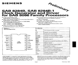
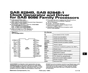
8284A-1 @ 30% Less Power Supply Current than Standard SAB 8284A, SAB 8284A-1 Generates the System clock for SAB 8086 and SAB 8088 Processors: upto 8 MHz with SAB 8284B upto 10 MHz with SAB 8284B-1 @ Uses a Crystal or a TTL Signal for Frequency Source upto 30 MHz @ Provides Synchronization for Synchronous and Asynchronous READY Signals @ 18-Pin Package @ Single +5V Power Supply Generates System Reset Output from Schmitt Trigger Input @ Capable of Clock Synchronization with Other SAB 8284Bs Figure 1 Pin Configuration cysnc (1 ad 18] Mec PCLK [2 7X AEN, (13 16 [_] X2 RDY, [}4 15] ASYNC READY (5 aaa8 14 (J EFI RDY, (16 BOE AEN, C7 12{_] osc CLK 8 1 _]RES GND 43 10 [RESET Pin Names x Connections for crystal F/C Clock source select EFI External clock input CSYNC Clock synchronization input ASYNC Ready synchronization select RDY, RDY, Ready signal EN Address enabled qualifiers for RDY,. RES Reset input RESET Synchronized reset output Osc Oscillator output CLK MOS Clock for the processor PCL
 14 Pages, 423 KB, Scan
8284A-1 30% Less Power Supply Current than Standard SAB 8284A, SAB 8284A-1 @ Generates the System clock for SAB 8086 and SAB 8088 Processors: upto 8 MHz with SAB 8284B upto 10 MHz with SAB 8284B-1 @ Uses a Crystal ora TTL Signal for Frequency Source upto 30 MHz Provides Synchronization for Synchronous and Asynchronous READY Signals 18-Pin Package Single +5V Power Supply Generates System Reset Output from Schmitt Trigger Input @ Capable of Clock Synchronization with Other SAB 8284Bs Figure 1 Pin Names Pin Configuration x Connections for crystal 2 F/C Clock source setect J EFI External clock input CYSNC C 1 18 a vec CSYNC Clock synchronization input PCLK [12 71] xX ASYNC Ready synchronization select tE0 RDY AEN, CL 3 16 td Xo RDY, Ready signal ROY; [| 4 SAB 15 LU ASYNC aEN, Address enabled qualifiers for RDY, READY |_j5 14 |_) EFI _ U 82848 I) RES Reset input ROY L 6 5 L] FIC RESET Synchronized reset output AEN L]7 12{ Jose OSC Oscillator output CLK Lo 8 N | RES CLK MOS Clock for the p
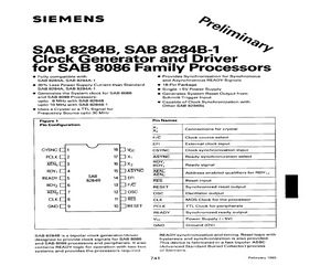 14 Pages, 248 KB, Scan
8284A-1 @ 30% Less Power Supply Current than Standard SAB 8284A, SAB 8284A-1 Generates the System clock for SAB 8086 and SAB 8088 Processors: upto 8 MHz with SAB 8284B upto 10 MHz with SAB 8284B-1 @ Uses a Crystal or a TTL Signal for Frequency Source upto 30 MHz @ Provides Synchronization for Synchronous and Asynchronous READY Signals , @ 18-Pin Package @ Single +5V Power Supply Generates System Reset Output from Schmitt Trigger Input @ Capable of Clock Synchronization with Other SAB 8284Bs Figure 1 Pin Configuration CYSNC (1 181] Ke PCLK (2 7x AEN, (43 16) x, ROY, (] 4 15{_] ASYNC READY (]5 ea8 14 (er I ROY, (46 BLIFE AEN, (7 12{_] OSC ciK 8 11 LJ RES GNO (9 10 [JRESET Pin Names x Connections for crystal F/T Clock source select EFI External clock input CSYNC Clock synchronization input ASYNT Ready synchronization select RDY, RDY, Ready signal a Address enabled qualifiers for RDY,2 2 RES Reset input RESET Synchronized reset output osc Oscillator output CLK MOS Clock for the processor
 13 Pages, 262 KB, Scan


