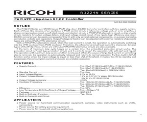
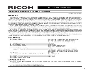
UT(mA) 1.850 1.750 0.1 L=10H 1.850 Output Voltage VOUT(V) Output Voltage VOUT(V) 1.850 VIN5V 1 10 100 1000 Output Current lOUT(mA) 10000 1.830 1.810 1.790 VIN3.3V VIN5V 1.770 VIN12V 1.750 0.1 1 10 100 1000 10000 Output Current lOUT(mA) 15 R1224N L=10H R1224N332F 3.400 3.38 3.380 Output Voltage VOUT(V) Output Voltage VOUT(V) R1224N332E 3.40 3.36 3.34 3.32 3.30 3.28 3.26 VIN4.8V 3.24 VIN7V 3.22 3.20 0.1 3.360 3.340 3.320 3.300 3.280 3.260 VIN4.8V 3.240 VIN7V 3.220 1 10 100 1000 3.200 0.1 10000 Output Current lOUT(mA) R1224N332G L=10H Output Voltage VOUT(V) Output Voltage VOUT(V) 3.360 1000 10000 3.340 3.320 3.300 3.280 VIN4.8V 3.260 VIN12V 3.240 VIN15V 1 10 100 1000 3.34 3.33 3.32 3.31 3.30 0.1 10000 Output Current lOUT(mA) 1 10 100 1000 10000 Output Current lOUT(mA) R1224N332G (VIN=16V) R1224N332H 3.35 L=10H Output Voltage VOUT(V) 3.400 3.34 3.33 3.32 3.31 3.380 3.360 3.340 3.320 3.300 3.280 VIN4.8V 3.260 VIN12V 3.240 VIN15V 3.220 1 10 100 1000 O
 40 Pages, 437 KB, Original
tput Voltage Vout (V) L=10uH 1.850 1.830 1.810 1.790 Vin3.3V 1.770 Vin5V 1.830 1.810 1.790 Vin3.3V Vin5V 1.770 Vin12V 1.750 1.750 0.1 1 10 100 1000 10000 Output Current Iout (mA) Rev. 1.11 0.1 1 10 100 1000 Output Current Iout (mA) - 11 - 10000 L=10uH R1224N332F 3.400 3.38 3.380 3.36 3.360 Output Voltage Vout (V) Output Voltage Vout (V) R1224N332E 3.40 3.34 3.32 3.30 3.28 Vin4.8V 3.26 Vin7V 3.24 3.340 3.320 3.300 3.280 3.240 3.220 3.20 3.200 1 10 100 1000 Output Current Iout (mA) R1224N332G Vin4.8V 3.260 3.22 0.1 L=10uH Vin7V 0.1 10000 L=10uH 1 10 100 1000 Output Current Iout (mA) 10000 R1224N332G(V IN =10V) 3.35 3.400 OUT(V) 3.360 3.340 Output Voltage V Output Voltage Vout (V) 3.380 3.320 3.300 3.280 3.260 Vin4.8V 3.240 Vin12V 3.220 Vin15V 3.34 3.33 3.32 3.31 3.30 3.200 0.1 1 10 100 1000 0.1 10000 1 10 100 1000 10000 Output Current I OUT(mA) Output Current Iout (mA) R1224N332H R1224N332G(V IN =16V) L=10uH 3.400 3.35 3.380 Output Vo
 35 Pages, 438 KB, Original
4N33 OPIA2110, OPIA2210, OPIA5010, OPIA6010 SMD and SOP Packages 5 Pin Features: * * * * 3,750 or 5,000 Vrms electrical isolation Choice of a Single and Dual LED Phototransistor or Photo Darlington Sensor Low-cost plastic Dual-In-Line (DIP) package Agency Approvals: * * UL Certification No: E58730 VDE No: 40026624,40026625 6 Pin Description: The OPIA series optocouplers are designed for applications that use an analog output (Phototransistor or Photo Darlington) in a dual-in-line package. A wide selection of configurations are available. With typical isolation voltage of 3,750 or 5,000 Volts(RMS), these product meet typical power system isolation requirements. Theory of operation: The LED transmitter is used to illuminate the Photosensor providing electrical isolation between two power systems while maintaining the ability to transmit information from one power system to the other. In many applications, analog signal levels may be required to be transmitted between two power systems while maintai
 23 Pages, 2041 KB, Original
UT(mA) 1.850 1.750 0.1 L=10H 1.850 Output Voltage VOUT(V) Output Voltage VOUT(V) 1.850 VIN5V 1 10 100 1000 Output Current lOUT(mA) 10000 1.830 1.810 1.790 VIN3.3V VIN5V 1.770 VIN12V 1.750 0.1 1 10 100 1000 10000 Output Current lOUT(mA) 15 R1224N L=10H R1224N332F 3.400 3.38 3.380 Output Voltage VOUT(V) Output Voltage VOUT(V) R1224N332E 3.40 3.36 3.34 3.32 3.30 3.28 3.26 VIN4.8V 3.24 VIN7V 3.22 3.20 0.1 3.360 3.340 3.320 3.300 3.280 3.260 VIN4.8V 3.240 VIN7V 3.220 1 10 100 1000 3.200 0.1 10000 Output Current lOUT(mA) R1224N332G L=10H Output Voltage VOUT(V) Output Voltage VOUT(V) 3.360 1000 10000 3.340 3.320 3.300 3.280 VIN4.8V 3.260 VIN12V 3.240 VIN15V 1 10 100 1000 3.34 3.33 3.32 3.31 3.30 0.1 10000 Output Current lOUT(mA) 1 10 100 1000 10000 Output Current lOUT(mA) R1224N332G (VIN=16V) R1224N332H 3.35 L=10H Output Voltage VOUT(V) 3.400 3.34 3.33 3.32 3.31 3.380 3.360 3.340 3.320 3.300 3.280 VIN4.8V 3.260 VIN12V 3.240 VIN15V 3.220 1 10 100 1000 O
 42 Pages, 1072 KB, Original
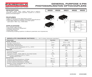
4N33 General Purpose 6-Pin Photodarlington Optocoupler Features Description High sensitivity to low input drive current The 4N29, 4N30, 4N31, 4N32, 4N33 have a gallium arsenide infrared emitter optically coupled to a silicon planar photodarlington. Meets or exceeds all JEDEC Registered Specifications tm VDE 0884 approval available as a test option - add option .300. (e.g., 4N29.300) Applications Low power logic circuits Telecommunications equipment Portable electronics Solid state relays Interfacing coupling systems of different potentials and impedances Packages Schematic White Package (-M Suffix) ANODE 1 6 1 6 BASE 6 1 CATHODE 2 5 COLLECTOR 6 1 N/C 3 4 EMITTER Black Package (No -M Suffix) 6 1 6 1 6 1 (c)2006 Fairchild Semiconductor Corporation 4N29, 4N30, 4N31, 4N32, 4N33 Rev. 1.0.1 www.fairchildsemi.com 4N29, 4N30, 4N31, 4N32, 4N33 General Purpose 6-Pin Photodarlington Optocoupler April 2007 Symbol Parameter Device Value Units C TOTAL DEVICE TSTG Storage
 13 Pages, 226 KB, Original
.850 Output Voltage Vout(V) 1.850 1.810 1.790 Vin3.3V 1.770 Vin5V L=27uH 1.810 1.790 Vin3.3V Vin5V 1.770 Vin12V 1.750 1.750 0.1 1 10 100 1000 10000 0.1 1 10 100 1000 10000 Output Current Iout (mA) Output Current Iout (mA) 12345 Rev. 1.11 - 11 - L=10uH R1224N332F 3.400 3.38 3.380 3.36 3.360 3.34 3.340 Output Voltage Vout (V) Output Voltage Vout (V) R1224N332E 3.40 3.32 3.30 3.28 Vin4.8V 3.26 Vin7V 3.24 3.320 3.300 3.280 3.260 Vin4.8V 3.240 Vin7V 3.220 3.22 L=10uH 3.200 3.20 0.1 1 10 100 1000 Output Current Iout (mA) R1224N332G 0.1 10000 L=10uH 1 10 100 1000 Output Current Iout (mA) 10000 R1224N332G(V IN =10V) 3.400 3.35 3.380 OUT(V) 3.340 3.34 3.33 3.320 Output Voltage V Output Voltage Vout (V) 3.360 3.300 3.280 3.260 Vin4.8V 3.240 Vin12V 3.220 Vin15V 3.32 3.31 3.30 3.200 0.1 1 10 100 1000 0.1 10000 1 10 100 1000 10000 Output Current I OUT(mA) Output Current Iout (mA) R1224N332H R1224N332G(V IN =16V) L=10uH 3.400 3.35 3.380 3.360 Out
 35 Pages, 394 KB, Original
e Transistor 4N28 (SHORT) Single Transistor 4N29 (SHORT) Darlington Transistor 4N29A (SHORT) Darlington Transistor 4N30 (SHORT) Darlington Transistor 4N31 (SHORT) Darlington Transistor 4N32 (SHORT) Darlington Transistor 4N32A (SHORT) Darlington Transistor 4N33 (SHORT) Darlington Transistor 4N35 (SHORT) Single Transistor 4N36 (SHORT) Single Transistor 4N37 (SHORT) Single Transistor 4N38 (SHORT) Single Transistor 4N38A (SHORT) Single Transistor 6N135 Photo IC 6N136 Photo IC 6N137 Photo IC 6N138 Photo IC 6N139 Photo IC CNY17-2 Single Transistor CNY17-3 Single Transistor CNY17-4 Single Transistor TLP112 Photo IC, Mini Flat TLP112A Photo IC, Mini Flat TLP113 Photo IC, Mini Flat TLP114A Photo IC, Mini Flat TLP114A(IGM) Photo IC, Mini Flat TLP115 Photo IC, Mini Flat TLP115A Photo IC, Mini Flat TLP151 Photo IC TLP124 Single Transistor, Mini Flat TLP126 Single Transistor, Mini Flat Darlington Transistor, Mini Flat TLP127 TLP130 Single Transistor, Mini Flat TLP131 Single Transistor, Mini Flat Single Transi
 61 Pages, 1092 KB, Original
4N33 have a gallium arsenide infrared emitter optically coupled to a silicon planar photodarlington. 4N29 4N30 4N31 4N32 4N33 FEATURES * High sensitivity to low input drive current * Meets or exceeds all JEDEC Registered Specifications * VDE 0884 approval available as a test option -add option .300. (e.g., 4N29.300) SCHEMATIC ANODE 1 6 BASE APPLICATIONS * * * * * Low power logic circuits Telecommunications equipment Portable electronics Solid state relays Interfacing coupling systems of different potentials and impedances. ABSOLUTE MAXIMUM RATINGS CATHODE 2 5 COLLECTOR N/C 3 4 EMITTER (TA = 25C Unless otherwise specified.) Parameter Symbol Value Units TSTG -55 to +150 C Operating Temperature TOPR -55 to +100 C Lead Solder Temperature TSOL 260 for 10 sec C 250 mW 3.3 mW/C IF 80 mA VR 3 V TOTAL DEVICE Storage Temperature Total Device Power Dissipation @ TA = 25C Derate above 25C EMITTER Continuous Forward Current Reverse Voltage Forward Current - Peak (300 s, 2% Duty Cycle) PD 3.0 A 15
 10 Pages, 201 KB, Original
UT(mA) 1.850 1.750 0.1 L=10H 1.850 Output Voltage VOUT(V) Output Voltage VOUT(V) 1.850 VIN5V 1 10 100 1000 Output Current lOUT(mA) 10000 1.830 1.810 1.790 VIN3.3V VIN5V 1.770 VIN12V 1.750 0.1 1 10 100 1000 10000 Output Current lOUT(mA) 15 R1224N L=10H R1224N332F 3.400 3.38 3.380 Output Voltage VOUT(V) Output Voltage VOUT(V) R1224N332E 3.40 3.36 3.34 3.32 3.30 3.28 3.26 VIN4.8V 3.24 VIN7V 3.22 3.20 0.1 3.360 3.340 3.320 3.300 3.280 3.260 VIN4.8V 3.240 VIN7V 3.220 1 10 100 1000 3.200 0.1 10000 Output Current lOUT(mA) R1224N332G L=10H Output Voltage VOUT(V) Output Voltage VOUT(V) 3.360 1000 10000 3.340 3.320 3.300 3.280 VIN4.8V 3.260 VIN12V 3.240 VIN15V 1 10 100 1000 3.34 3.33 3.32 3.31 3.30 0.1 10000 Output Current lOUT(mA) 1 10 100 1000 10000 Output Current lOUT(mA) R1224N332G (VIN=16V) R1224N332H 3.35 L=10H Output Voltage VOUT(V) 3.400 3.34 3.33 3.32 3.31 3.380 3.360 3.340 3.320 3.300 3.280 VIN4.8V 3.260 VIN12V 3.240 VIN15V 3.220 1 10 100 1000 O
 42 Pages, 904 KB, Original
4N33 General Purpose 6-Pin Photodarlington Optocoupler Features Description High sensitivity to low input drive current The 4N29, 4N30, 4N31, 4N32, 4N33 have a gallium arsenide infrared emitter optically coupled to a silicon planar photodarlington. Meets or exceeds all JEDEC Registered Specifications tm VDE 0884 approval available as a test option - add option .300. (e.g., 4N29.300) Applications Low power logic circuits Telecommunications equipment Portable electronics Solid state relays Interfacing coupling systems of different potentials and impedances Packages Schematic White Package (-M Suffix) ANODE 1 6 1 6 BASE 6 1 CATHODE 2 5 COLLECTOR 6 1 N/C 3 4 EMITTER Black Package (No -M Suffix) 6 1 6 1 6 1 (c)2006 Fairchild Semiconductor Corporation 4N29, 4N30, 4N31, 4N32, 4N33 Rev. 1.0.1 www.fairchildsemi.com 4N29, 4N30, 4N31, 4N32, 4N33 General Purpose 6-Pin Photodarlington Optocoupler April 2007 Symbol Parameter Device Value Units C TOTAL DEVICE TSTG Storage
 17 Pages, 360 KB, Original
UT(mA) 1.850 1.750 0.1 L=10H 1.850 Output Voltage VOUT(V) Output Voltage VOUT(V) 1.850 VIN5V 1 10 100 1000 Output Current lOUT(mA) 10000 1.830 1.810 1.790 VIN3.3V VIN5V 1.770 VIN12V 1.750 0.1 1 10 100 1000 10000 Output Current lOUT(mA) 15 R1224N L=10H R1224N332F 3.400 3.38 3.380 Output Voltage VOUT(V) Output Voltage VOUT(V) R1224N332E 3.40 3.36 3.34 3.32 3.30 3.28 3.26 VIN4.8V 3.24 VIN7V 3.22 3.20 0.1 3.360 3.340 3.320 3.300 3.280 3.260 VIN4.8V 3.240 VIN7V 3.220 1 10 100 1000 3.200 0.1 10000 Output Current lOUT(mA) R1224N332G L=10H Output Voltage VOUT(V) Output Voltage VOUT(V) 3.360 1000 10000 3.340 3.320 3.300 3.280 VIN4.8V 3.260 VIN12V 3.240 VIN15V 1 10 100 1000 3.34 3.33 3.32 3.31 3.30 0.1 10000 Output Current lOUT(mA) 1 10 100 1000 10000 Output Current lOUT(mA) R1224N332G (VIN=16V) R1224N332H 3.35 L=10H Output Voltage VOUT(V) 3.400 3.34 3.33 3.32 3.31 3.380 3.360 3.340 3.320 3.300 3.280 VIN4.8V 3.260 VIN12V 3.240 VIN15V 3.220 1 10 100 1000 O
 40 Pages, 351 KB, Original
oltage Vout (V) L=10uH 1.850 1.830 1.810 1.790 Vin3.3V 1.770 Vin5V 1.830 1.810 1.790 Vin3.3V Vin5V 1.770 Vin12V 1.750 1.750 0.1 1 10 100 1000 Output Current Iout (mA) 10000 0.1 1 10 100 1000 Output Current Iout (mA) 10000 12345 Rev. 1.12 - 12 - L=10uH R1224N332F 3.400 3.38 3.380 3.36 3.360 Output Voltage Vout (V) Output Voltage Vout (V) R1224N332E 3.40 3.34 3.32 3.30 3.28 Vin4.8V 3.26 Vin7V 3.24 3.340 3.320 3.300 3.280 3.240 3.220 3.20 3.200 1 10 100 1000 Output Current Iout (mA) R1224N332G Vin4.8V 3.260 3.22 0.1 L=10uH Vin7V 0.1 10000 L=10uH 1 10 100 1000 Output Current Iout (mA) 10000 R1224N332G(V IN =10V) 3.35 3.400 OUT(V) 3.360 3.340 Output Voltage V Output Voltage Vout (V) 3.380 3.320 3.300 3.280 3.260 Vin4.8V 3.240 Vin12V 3.220 Vin15V 3.34 3.33 3.32 3.31 3.30 3.200 0.1 1 10 100 1000 0.1 10000 1 10 100 1000 10000 Output Current I OUT(mA) Output Current Iout (mA) R1224N332H R1224N332G(V IN =16V) L=10uH 3.400 3.35 3.380 3.34 Outp
 36 Pages, 494 KB, Original
UT(mA) 1.850 1.750 0.1 L=10H 1.850 Output Voltage VOUT(V) Output Voltage VOUT(V) 1.850 VIN5V 1 10 100 1000 Output Current lOUT(mA) 10000 1.830 1.810 1.790 VIN3.3V VIN5V 1.770 VIN12V 1.750 0.1 1 10 100 1000 10000 Output Current lOUT(mA) 15 R1224N L=10H R1224N332F 3.400 3.38 3.380 Output Voltage VOUT(V) Output Voltage VOUT(V) R1224N332E 3.40 3.36 3.34 3.32 3.30 3.28 3.26 VIN4.8V 3.24 VIN7V 3.22 3.20 0.1 3.360 3.340 3.320 3.300 3.280 3.260 VIN4.8V 3.240 VIN7V 3.220 1 10 100 1000 3.200 0.1 10000 Output Current lOUT(mA) R1224N332G L=10H Output Voltage VOUT(V) Output Voltage VOUT(V) 3.360 1000 10000 3.340 3.320 3.300 3.280 VIN4.8V 3.260 VIN12V 3.240 VIN15V 1 10 100 1000 3.34 3.33 3.32 3.31 3.30 0.1 10000 Output Current lOUT(mA) 1 10 100 1000 10000 Output Current lOUT(mA) R1224N332G (VIN=16V) R1224N332H 3.35 L=10H Output Voltage VOUT(V) 3.400 3.34 3.33 3.32 3.31 3.380 3.360 3.340 3.320 3.300 3.280 VIN4.8V 3.260 VIN12V 3.240 VIN15V 3.220 1 10 100 1000 O
 40 Pages, 441 KB, Original
UT(mA) 1.850 1.750 0.1 L=10H 1.850 Output Voltage VOUT(V) Output Voltage VOUT(V) 1.850 VIN5V 1 10 100 1000 Output Current lOUT(mA) 10000 1.830 1.810 1.790 VIN3.3V VIN5V 1.770 VIN12V 1.750 0.1 1 10 100 1000 10000 Output Current lOUT(mA) 15 R1224N L=10H R1224N332F 3.400 3.38 3.380 Output Voltage VOUT(V) Output Voltage VOUT(V) R1224N332E 3.40 3.36 3.34 3.32 3.30 3.28 3.26 VIN4.8V 3.24 VIN7V 3.22 3.20 0.1 3.360 3.340 3.320 3.300 3.280 3.260 VIN4.8V 3.240 VIN7V 3.220 1 10 100 1000 3.200 0.1 10000 Output Current lOUT(mA) R1224N332G L=10H Output Voltage VOUT(V) Output Voltage VOUT(V) 3.360 1000 10000 3.340 3.320 3.300 3.280 VIN4.8V 3.260 VIN12V 3.240 VIN15V 1 10 100 1000 3.34 3.33 3.32 3.31 3.30 0.1 10000 Output Current lOUT(mA) 1 10 100 1000 10000 Output Current lOUT(mA) R1224N332G (VIN=16V) R1224N332H 3.35 L=10H Output Voltage VOUT(V) 3.400 3.34 3.33 3.32 3.31 3.380 3.360 3.340 3.320 3.300 3.280 VIN4.8V 3.260 VIN12V 3.240 VIN15V 3.220 1 10 100 1000 O
 42 Pages, 401 KB, Original
1.790 VIN3.3V 1.770 VIN5V 1 10 100 1000 Output Current lOUT(mA) 16 10 1.850 1.830 1.750 0.1 1 Output Current IOUT(mA) 1.850 1.750 0.1 VIN5V 10000 1.830 1.810 1.790 VIN3.3V VIN5V 1.770 VIN12V 1.750 0.1 1 10 100 1000 Output Current lOUT(mA) 10000 R1224N R1224N332F L=10uH 3.400 3.38 3.380 Output Voltage VOUT(V) Output Voltage VOUT(V) R1224N332E L=10uH 3.40 3.36 3.34 3.32 3.30 3.28 3.26 VIN4.8V 3.24 VIN7V 3.22 3.20 0.1 3.360 3.340 3.320 3.300 3.280 3.260 VIN4.8V 3.240 VIN7V 3.220 1 10 100 1000 3.200 0.1 10000 Output Current lOUT(mA) R1224N332G L=10uH Output Voltage VOUT(V) Output Voltage VOUT(V) 1000 10000 R1224N332G (VIN=10V) 3.360 3.340 3.320 3.300 3.280 VIN4.8V 3.260 VIN12V 3.240 VIN15V 3.220 1 10 100 1000 3.34 3.33 3.32 3.31 3.30 0.1 10000 Output Current lOUT(mA) 1 10 100 1000 10000 Output Current lOUT(mA) R1224N332G (VIN=16V) R1224N332H L=10uH 3.35 3.400 Output Voltage VOUT(V) Output Voltage VOUT(V) 100 3.35 3.380 3.34 3.33 3.32 3.
 40 Pages, 316 KB, Original


