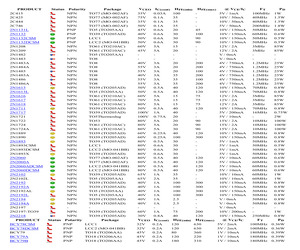
42.1nC 42.1nC 42nC 42nC 42nC QG (nC) 42nC 33nC 33nC 33nC 33.5nC 33nC 33nC 29.5nC 30nC 30nC 30nC 30nC 30nC 30nC 29nC 31nC 2N6845 2N6845LCC4 2N6845U 2N6847 2N6847U 2N6849 2N6849L 2N6849LCC4 2N6849U 2N6849U5 2N6851 2N6851LCC4 2N6851U 2N6851U5 2N6851X 2N6896 2N7000CSM 2N7002CSM 2N7002DCSM 2N7075 2N7077 2N7081-220M PRODUCT 2N7081-220M-ISO 2N7081-257-F 2N7081SMM 2N7085 2N7085-257-F 2N7085-F 2N7085SMM 2N7086 2N7086-257-F 2N7086-F 2N7086SMM 2N7089 2N7089-257-F 2N7089-F 2N7089SMM 2N7090 2N7091 2N7091-257-F 2N7091-F 2N7091SMM 2N7092 2N7218 2N7218SMD 2N7218U 2N7218U1 2N7219 2N7219SMD 2N7219U 2N7219U1 2N7220 2N7221 2N7221SMD 2N7221U P-Channel P-Channel P-Channel P-Channel P-Channel P-Channel P-Channel P-Channel P-Channel P-Channel P-Channel P-Channel P-Channel P-Channel P-Channel P-Channel N-Channel N-Channel Dual N-Channel N-Channel Status Polarity N-Channel N-Channel N-Channel N-Channel N-Channel N-Channel N-Channel N-Channel N-Channel N-Channel N-Channel N-Channel N-Channel N-Channel P-Channel P-Channel
 1197 Pages, 40410 KB, Original
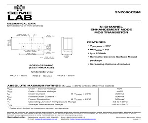
2N7000CSM MECHANICAL DATA Dimensions in mm (inches) N-CHANNEL ENHANCEMENT MODE MOS TRANSISTOR 0.31 rad. (0.012) 3 FEATURES 2 0.76 0.15 (0.03 0.006) 2.54 0.13 (0.10 0.005) 0.51 0.10 (0.02 0.004) 1 1.91 0.10 (0.075 0.004) * V(BR)DSS = 60V * RDS(ON) = 5 A 0.31 rad. (0.012) 3.05 0.13 (0.12 0.005) A= * ID = 200mA 1.40 (0.055) max. 1.02 0.10 (0.04 0.004) * Hermetic Ceramic Surface Mount package * Screening Options Available SOT23 CERAMIC (LCC1 PACKAGE) Underside View PAD 1 - Gate PAD 2 - Source PAD 3 - Drain ABSOLUTE MAXIMUM RATINGS (TCASE = 25C unless otherwise stated) VDS Drain - Source Voltage 60V VGS Gate - Source Voltage 40V ID Drain Current IDM Pulsed Drain Current * PD Power Dissipation Tj Operating Junction Temperature Range -55 to 150C Tstg Storage Temperature Range -55 to 150C @ TCASE = 25C 200mA 500mA @ TCASE = 25C 300mW * Pulse width limited by maximum junction temperature. Semelab Plc reserves the right to change test conditions, parameter limits and package dimensions without notice. Info
 2 Pages, 31 KB, Original
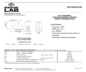
2N7000CSM MECHANICAL DATA Dimensions in mm (inches) N-CHANNEL ENHANCEMENT MODE MOS TRANSISTOR 0.31 rad. (0.012) 3 FEATURES 2 0.76 0.15 (0.03 0.006) 2.54 0.13 (0.10 0.005) 0.51 0.10 (0.02 0.004) 1 1.91 0.10 (0.075 0.004) * V(BR)DSS = 60V * RDS(ON) = 5W A 0.31 rad. (0.012) 3.05 0.13 (0.12 0.005) A= * ID = 200mA 1.40 (0.055) max. 1.02 0.10 (0.04 0.004) * Hermetic Ceramic Surface Mount package * Screening Options Available SOT23 CERAMIC (LCC1 PACKAGE) Underside View PAD 1 - Gate PAD 2 - Source PAD 3 - Drain ABSOLUTE MAXIMUM RATINGS (TCASE = 25C unless otherwise stated) VDS Drain - Source Voltage 60V VGS Gate - Source Voltage 40V ID Drain Current IDM Pulsed Drain Current * PD Power Dissipation Tj Operating Junction Temperature Range -55 to 150C Tstg Storage Temperature Range -55 to 150C @ TCASE = 25C 200mA 500mA @ TCASE = 25C 300mW * Pulse width limited by maximum junction temperature. Magnatec. Telephone +44(0)1455 554711. Fax +44(0)1455 558843. E-mail: magnatec@semelab.co.uk Website: http://www.seme
 2 Pages, 19 KB, Original


