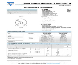
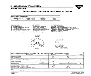
2N6660JANTX, 2N6660JANTXV www.vishay.com Vishay Siliconix N-Channel 60 V (D-S) MOSFET FEATURES PRODUCT SUMMARY VDS (V) 60 RDS(on) () at VGS = 10 V 3 Configuration * Military Qualified * * * * * Single TO-205AD (TO-39) BENEFITS * * * * * * S 1 2 Low On-Resistence: 1.3 Low Threshold: 1.7 V Low Input Capacitance: 35 pF Fast Switching Speed: 8 ns Low Input and Output Leakage APPLICATIONS 3 G Guaranteed Reliability Low Offset Voltage Low-Voltage Operation Easily Driven Without Buffer High-Speed Circuits Low Error Voltage * Hi-Rel Systems * Direct Logic-Level Interface: TTL/CMOS * Drivers: Relays, Solenoids, Lamps, Hammers, Displays, Memories, Transistors, etc. * Battery Operated Systems * Solid-State Relays D Top View ORDERING INFORMATION PART DESCRIPTION/DSCC PART NUMBER PACKAGE 2N6660 2N6660-2 2N6660JANTX VISHAY ORDERING PART NUMBER Commercial 2N6660 Commercial, Lead (Pb)-free 2N6660-E3 www.vishay.com/doc?67884 See -2 Flow Document 2N6660-2 JANTX2N6660 (std Au leads)
 7 Pages, 121 KB, Original
2N6660JANTX, 2N6660JANTXV www.vishay.com Vishay Siliconix N-Channel 60 V (D-S) MOSFET FEATURES PRODUCT SUMMARY VDS (V) 60 RDS(on) () at VGS = 10 V 3 Configuration * Military Qualified * * * * * Single TO-205AD (TO-39) BENEFITS * * * * * * S 1 2 Low On-Resistence: 1.3 Low Threshold: 1.7 V Low Input Capacitance: 35 pF Fast Switching Speed: 8 ns Low Input and Output Leakage APPLICATIONS 3 G Guaranteed Reliability Low Offset Voltage Low-Voltage Operation Easily Driven Without Buffer High-Speed Circuits Low Error Voltage * Hi-Rel Systems * Direct Logic-Level Interface: TTL/CMOS * Drivers: Relays, Solenoids, Lamps, Hammers, Displays, Memories, Transistors, etc. * Battery Operated Systems * Solid-State Relays D Top View ORDERING INFORMATION PART DESCRIPTION/DSCC PART NUMBER PACKAGE 2N6660 2N6660-2 2N6660JANTX VISHAY ORDERING PART NUMBER Commercial 2N6660 Commercial, Lead (Pb)-free 2N6660-E3 www.vishay.com/doc?67884 See -2 Flow Document 2N6660-2 JANTX2N6660 (std Au leads)
 6 Pages, 127 KB, Original
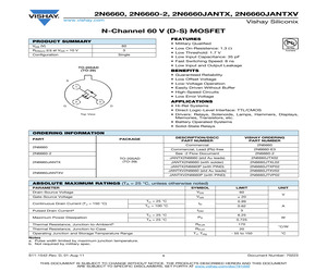
2N6660JANTX, 2N6660JANTXV www.vishay.com Vishay Siliconix N-Channel 60 V (D-S) MOSFET FEATURES PRODUCT SUMMARY VDS (V) 60 RDS(on) () at VGS = 10 V 3 Configuration * Military Qualified * * * * * Single TO-205AD (TO-39) BENEFITS * * * * * * S 1 2 Low On-Resistence: 1.3 Low Threshold: 1.7 V Low Input Capacitance: 35 pF Fast Switching Speed: 8 ns Low Input and Output Leakage APPLICATIONS 3 G Guaranteed Reliability Low Offset Voltage Low-Voltage Operation Easily Driven Without Buffer High-Speed Circuits Low Error Voltage * Hi-Rel Systems * Direct Logic-Level Interface: TTL/CMOS * Drivers: Relays, Solenoids, Lamps, Hammers, Displays, Memories, Transistors, etc. * Battery Operated Systems * Solid-State Relays D Top View ORDERING INFORMATION PART DESCRIPTION/DSCC PART NUMBER PACKAGE 2N6660 2N6660-2 2N6660JANTX VISHAY ORDERING PART NUMBER Commercial 2N6660 Commercial, Lead (Pb)-free 2N6660-E3 www.vishay.com/doc?67884 See -2 Flow Document 2N6660-2 JANTX2N6660 (std Au leads)
 6 Pages, 119 KB, Original
2N6660JANTX, 2N6660JANTXV www.vishay.com Vishay Siliconix N-Channel 60 V (D-S) MOSFET FEATURES PRODUCT SUMMARY VDS (V) 60 RDS(on) () at VGS = 10 V 3 Configuration * Military Qualified * * * * * Single TO-205AD (TO-39) BENEFITS * * * * * * S 1 2 Low On-Resistence: 1.3 Low Threshold: 1.7 V Low Input Capacitance: 35 pF Fast Switching Speed: 8 ns Low Input and Output Leakage APPLICATIONS 3 G Guaranteed Reliability Low Offset Voltage Low-Voltage Operation Easily Driven Without Buffer High-Speed Circuits Low Error Voltage * Hi-Rel Systems * Direct Logic-Level Interface: TTL/CMOS * Drivers: Relays, Solenoids, Lamps, Hammers, Displays, Memories, Transistors, etc. * Battery Operated Systems * Solid-State Relays D Top View ORDERING INFORMATION PART DESCRIPTION/DSCC PART NUMBER PACKAGE 2N6660 2N6660-2 2N6660JANTX VISHAY ORDERING PART NUMBER Commercial 2N6660 Commercial, Lead (Pb)-free 2N6660-E3 www.vishay.com/doc?67884 See -2 Flow Document 2N6660-2 JANTX2N6660 (std Au leads)
 6 Pages, 128 KB, Original
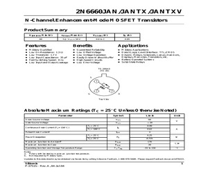
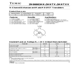
2N6660JAN/JANTX/JANTXV N-Channel Enhancement-Mode MOSFET Transistors Product Summary V(BR)DSS Min (V) rDS(on) Max () VGS(th) (V) ID (A) 60 3 @ VGS = 10 V 0.8 to 2 0.99 Features Benefits Applications Military Applications Direct Logic-Level Interface: TTL/CMOS Drivers: Relays, Solenoids, Lamps, Hammers, Displays, Memories, Transistors, etc. Battery Operated Systems Solid-State Relays Military Qualified Low On-Resistance: 1.3 Low Threshold: 1.7 V Low Input Capacitance: 35 pF Fast Switching Speed: 8 ns Low Input and Output Leakage Guaranteed Reliability Low Offset Voltage Low-Voltage Operation Easily Driven Without Buffer High-Speed Circuits Low Error Voltage TO-205AD (TO-39) S 1 2 3 G D Top View Absolute Maximum Ratings (TC = 25C Unless Otherwise Noted) Parameter Symbol Limit Drain-Source Voltage VDS 60 Gate-Source Voltage VGS 20 Continuous Drain Current (TJ = 150C) Pulsed Drain TC= 25C TC= 100C Currenta Power Dissipation TA= 25C 0.62 A 3 6.25 PD 0.725 Maximum Junction-to-Ambientb RthJA 170 Maximum
 2 Pages, 21 KB, Original
2N6660JAN/JANTX/JANTXV TEMIC Siliconix N-Channel Enhancement-Mode MOS Transistors Product Summary Vierypss Min (V) Tps(n) Max (2) Vesan) (Y) Ip (A) 60 3 @ Ves = 10 V 0.8 to 2 0.99 Features Benefits Applications Military Qualified @ Guaranteed Reliability @ Military Applications @ Low On-Resistance: 1.3 Q Low Offset Voltage @ Direct Logic-Level Interface: TTL/CMOS @ Low Threshold: 1.7V @ Low-Voltage Operation @ Drivers: Relays, Solenoids, Lamps, Hammers, @ Low Input Capacitance: 35 pF Easily Driven Without Buffer Displays, Memories, Transistors, etc. Fast Switching Speed: 8 ns High-Speed Circuits e Battery Operated Systems Low Input and Output Leakage Low Error Voltage @ Solid-State Relays TO-205AD (TO-39) Top View Absolute Maximum Ratings (Tc = 25C Unless Otherwise Noted) Parameter Symbol Limit Unit Drain-Source Voltage Vps 60 Vv Gate-Source Voltage Vos +20 Tc= 25C 0.99 Continuous Drain Current (Ty = 150C) Ip Tc= 100C 0.62 A Pulsed Drain Current? Ipm 3 Tc= 25C 6.25 Power Dissipation Pp Ww Ta= 25C
 2 Pages, 62 KB, Scan
2N6660JAN/JANTX/JANTXV [yy VISHAY Vishay Siliconix JAN Qualified N-Channel 60-V (D-S) MOSFETs PRODUCT SUMMARY Viaryoss Min (V) Tps(on) Max (Q) Vesithy (V) Ip (A) 60 3 @ Veg =10V 0.8to2 0.99 FEATURES BENEFITS APPLICATIONS e Military Qualified e@ Guaranteed Reliability e Military Applications Low On-Resistance: 1.3 Q Low Offset Voltage Direct Logic-Level inierface: TTL/CMOS @ Low Threshold: 1.7 V Low-Voltage Operation @ Drivers: Relays, Solenoids, Lamps, Hammers, @ Low Input Capacitance: 35 pF @ Easily Driven Without Buffer Displays, Memories, Transistors, etc. Fast Switching Speed: 8ns = _High-Speed Circuits Battery Operated Systems Low Input and Output Low Error Voltage Solid-State Relays Leakage TO-205AD (TO-39) Top View Device Marking Side View JAN2N6660* S" flixxyy S" = Siliconix Logo f= Factory Code 4 = Lot Traceability xxyy = Date Code Note: or JANTX2N6660 JANTXV2N6660 ABSOLUTE MAXIMUM RATINGS (T, = 25C UNLESS OTHERWISE NOTED) Parameter Symbol Limit Unit Drain-Source Voltage Vos 60 Vv Gate-S
 2 Pages, 59 KB, Scan
2N6660JAN/JANTX/JANTXV N-Channel Enhancement-Mode MOSFET Transistors Product Summary V(BR)DSS Min (V) rDS(on) Max () VGS(th) (V) ID (A) 60 3 @ VGS = 10 V 0.8 to 2 0.99 Features Benefits Applications Military Applications Direct Logic-Level Interface: TTL/CMOS Drivers: Relays, Solenoids, Lamps, Hammers, Displays, Memories, Transistors, etc. Battery Operated Systems Solid-State Relays Military Qualified Low On-Resistance: 1.3 Low Threshold: 1.7 V Low Input Capacitance: 35 pF Fast Switching Speed: 8 ns Low Input and Output Leakage Guaranteed Reliability Low Offset Voltage Low-Voltage Operation Easily Driven Without Buffer High-Speed Circuits Low Error Voltage TO-205AD (TO-39) S 1 2 3 G D Top View Absolute Maximum Ratings (TC = 25C Unless Otherwise Noted) Parameter Symbol Limit Drain-Source Voltage VDS 60 Gate-Source Voltage VGS 20 Continuous Drain Current (TJ = 150C) Pulsed Drain TC= 25C TC= 100C Currenta Power Dissipation TA= 25C 0.62 A 3 6.25 PD 0.725 Maximum Junction-to-Ambientb RthJA 170 Maximum
 2 Pages, 25 KB, Original
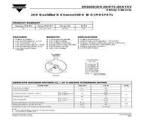
2N6660JAN/JANTX/JANTXV Vishay Siliconix JAN Qualified N-Channel 60-V (D-S) MOSFET PRODUCT SUMMARY V(BR)DSS Min (V) rDS(on) Max () VGS(th) (V) ID (A) 60 3 at VGS = 10 V 0.8 to 2 0.99 TO-205AD (TO-39) BENEFITS * Guaranteed Reliability * Low Offset Voltage * Low-Voltage Operation * Easily Driven Without Buffer * High-Speed Circuits * Low Error Voltage S 1 2 FEATURES * Military Qualified * Low On-Resistence: 1.3 * Low Threshold: 1.7 V * Low Input Capacitance: 35 pF * Fast Switching Speed: 8 ns * Low Input and Output Leakage APPLICATIONS * Military Applications * Direct Logic-Level Interface: TTL/CMOS * Drivers: Relays, Solenoids, Lamps, Hammers, Displays, Memories, Transistors, etc. * Battery Operated Systems * Solid-State Relays 3 G D Top View ABSOLUTE MAXIMUM RATINGS TA = 25 C, unless otherwise noted Parameter Symbol Limit Drain-Source Voltage VDS 60 Gate-Source Voltage VGS 20 Continuous Drain Current (TJ = 150 C) Pulsed Drain Current TC = 25 C TC = 100 C a IDM TC = 25 C Power Dissipation ID TA = 2
 3 Pages, 102 KB, Original
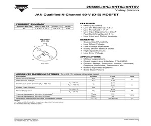
2N6660JAN/JANTX/JANTXV Vishay Siliconix JAN Qualified N-Channel 60-V (D-S) MOSFETs PRODUCT SUMMARY V(BR)DSS Min (V) rDS(on) Max (W) VGS(th) (V) ID (A) 60 3 @ VGS = 10 V 0.8 to 2 0.99 FEATURES BENEFITS APPLICATIONS D D D D D D D D D D D D D Military Applications D Direct Logic-Level Interface: TTL/CMOS D Drivers: Relays, Solenoids, Lamps, Hammers, Displays, Memories, Transistors, etc. D Battery Operated Systems D Solid-State Relays Military Qualified Low On-Resistance: 1.3 W Low Threshold: 1.7 V Low Input Capacitance: 35 pF Fast Switching Speed: 8 ns Low Input and Output Leakage Guaranteed Reliability Low Offset Voltage Low-Voltage Operation Easily Driven Without Buffer High-Speed Circuits Low Error Voltage TO-205AD (TO-39) Device Marking Side View S 1 JAN2N6660* "S" fllxxyy 2 "S" = Siliconix Logo f = Factory Code ll = Lot Traceability xxyy = Date Code 3 G D *Note: or JANTX2N6660 JANTXV2N6660 Top View ABSOLUTE MAXIMUM RATINGS (TA = 25_C UNLESS OTHERWISE NOTED) Parameter Symbol Limit Drain-Source V
 3 Pages, 49 KB, Original
2N6660JAN/JANTX/JANTXV Vishay Siliconix JAN Qualified N-Channel 60-V (D-S) MOSFETs PRODUCT SUMMARY V(BR)DSS Min (V) rDS(on) Max (W) VGS(th) (V) ID (A) 60 3 @ VGS = 10 V 0.8 to 2 0.99 FEATURES BENEFITS APPLICATIONS D D D D D D D D D D D D D Military Applications D Direct Logic-Level Interface: TTL/CMOS D Drivers: Relays, Solenoids, Lamps, Hammers, Displays, Memories, Transistors, etc. D Battery Operated Systems D Solid-State Relays Military Qualified Low On-Resistance: 1.3 W Low Threshold: 1.7 V Low Input Capacitance: 35 pF Fast Switching Speed: 8 ns Low Input and Output Leakage Guaranteed Reliability Low Offset Voltage Low-Voltage Operation Easily Driven Without Buffer High-Speed Circuits Low Error Voltage TO-205AD (TO-39) Device Marking Side View S 1 JAN2N6660* "S" fllxxyy 2 "S" = Siliconix Logo f = Factory Code ll = Lot Traceability xxyy = Date Code 3 G D *Note: or JANTX2N6660 JANTXV2N6660 Top View ABSOLUTE MAXIMUM RATINGS (TA = 25_C UNLESS OTHERWISE NOTED) Parameter Symbol Limit Drain-Source V
 2 Pages, 21 KB, Original
2N6660JAN/JANTX/JANTXV Vishay Siliconix JAN Qualified N-Channel 60-V (D-S) MOSFET PRODUCT SUMMARY V(BR)DSS Min (V) rDS(on) Max () VGS(th) (V) ID (A) 60 3 at VGS = 10 V 0.8 to 2 0.99 TO-205AD (TO-39) BENEFITS * Guaranteed Reliability * Low Offset Voltage * Low-Voltage Operation * Easily Driven Without Buffer * High-Speed Circuits * Low Error Voltage S 1 2 FEATURES * Military Qualified * Low On-Resistence: 1.3 * Low Threshold: 1.7 V * Low Input Capacitance: 35 pF * Fast Switching Speed: 8 ns * Low Input and Output Leakage APPLICATIONS * Military Applications * Direct Logic-Level Interface: TTL/CMOS * Drivers: Relays, Solenoids, Lamps, Hammers, Displays, Memories, Transistors, etc. * Battery Operated Systems * Solid-State Relays 3 G D Top View ABSOLUTE MAXIMUM RATINGS TA = 25 C, unless otherwise noted Parameter Symbol Limit Drain-Source Voltage VDS 60 Gate-Source Voltage VGS 20 Continuous Drain Current (TJ = 150 C) Pulsed Drain Current TC = 25 C TC = 100 C a IDM TC = 25 C Power Dissipation ID TA = 2
 3 Pages, 121 KB, Original
tion Technology Package EFR (ppm) 1.2 LFR (FIT) 1.2 TEMIC Semiconductors 07.97 Type Description 2N6659-2 Small Signal Mosfets N-LP-B TO39 AOQ (ppm) 2 2N6660 Small Signal Mosfets N-LP-B TO39 2 0.45 0.45 2N6660-2 Small Signal Mosfets N-LP-B TO39 2 0.45 0.45 2N6660JTV01 Small Signal Mosfets N-LP-B TO39 2 0.45 0.45 2N6660JTX01 Small Signal Mosfets N-LP-B TO39 2 0.45 0.45 2N6661 Small Signal Mosfets N-LP-B TO39 2 0.45 0.45 2N6661-2 Small Signal Mosfets N-LP-B TO39 2 0.45 0.45 2N6661-ER Small Signal Mosfets N-LP-B TO39 2 0.45 0.45 2N6661JAN01 Small Signal Mosfets N-LP-B TO39 2 0.45 0.45 2N6661JTV01 Small Signal Mosfets N-LP-B TO39 2 0.45 0.45 2N6661JTX01 Small Signal Mosfets N-LP-B TO39 2 0.45 0.45 2N6661JXTL01 Small Signal Mosfets N-LP-B TO39 2 0.45 0.45 2N6661L-2 Small Signal Mosfets N-LP-B TO39 2 0.45 0.45 2N7000 Small Signal Mosfets N-LP-B TO92 2 0.45 0.45 2N7000-18 Small Signal Mosfets N-LP-B TO92 2 0.45 0.45 2N7000-TA Small Signal Mosfets N-LP-B TO92 2 0.45 0.45 2N7000-TR1 Small Sign
 78 Pages, 680 KB, Original
2N6660JAN/JANTX/JANTXV Vishay Siliconix JAN Qualified N-Channel 60-V (D-S) MOSFETs PRODUCT SUMMARY V(BR)DSS Min (V) rDS(on) Max (W) VGS(th) (V) ID (A) 60 3 @ VGS = 10 V 0.8 to 2 0.99 FEATURES BENEFITS APPLICATIONS D D D D D D D D D D D D D Military Applications D Direct Logic-Level Interface: TTL/CMOS D Drivers: Relays, Solenoids, Lamps, Hammers, Displays, Memories, Transistors, etc. D Battery Operated Systems D Solid-State Relays Military Qualified Low On-Resistance: 1.3 W Low Threshold: 1.7 V Low Input Capacitance: 35 pF Fast Switching Speed: 8 ns Low Input and Output Leakage Guaranteed Reliability Low Offset Voltage Low-Voltage Operation Easily Driven Without Buffer High-Speed Circuits Low Error Voltage TO-205AD (TO-39) Device Marking Side View S 1 JAN2N6660* "S" fllxxyy 2 "S" = Siliconix Logo f = Factory Code ll = Lot Traceability xxyy = Date Code 3 G D *Note: or JANTX2N6660 JANTXV2N6660 Top View ABSOLUTE MAXIMUM RATINGS (TA = 25_C UNLESS OTHERWISE NOTED) Parameter Symbol Limit Drain-Source V
 3 Pages, 49 KB, Original


