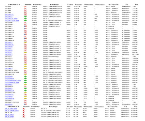
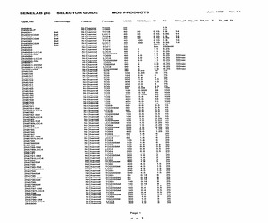
6AA) 40V 0.1A 0.36W 2N6659 N-Channel TO39 (TO205AD) 60V 1.1A 6.25W 5 2N6659LCC4 N-Channel LCC4 60V 1.1A 6.25W 5 2N6659SMD N-Channel SMD1 (TO276AB) 60V 1.1A 6.25W 5 2N6659U1 N-Channel SMD1 (TO276AB) 60V 1.1A 6.25W 5 2N6659U5 N-Channel LCC4 60V 1.1A 6.25W 5 2N6660 N-Channel TO39 (TO205AD) 60V 1A 5W 3 50pF 2N6660C4A N-Channel LCC4 60V 1A 5W 3 50pF 2N6660CSM4 N-Channel LCC3 (MO-041BA) 60V 1A 3W 3 50pF 2N6660Q Quad N-Channel LCC6 (MO-042AA) 60V 1.1A 6.25W 3 50pF 2N6661 N-Channel TO39 (TO205AD) 90V 0.9A 5W 4 50pF 2N6661-220M N-Channel TO257AB (TO220M) 90V 0.9A 6.25W 4 50pF 2N6661-220M-ISO N-Channel TO257AB (TO220M) 90V 0.9A 6.25W 4 50pF 2N6661CSM4 N-Channel LCC3 (MO-041BA) 90V 0.9A 6.25W 4 50pF 2N6661DCSM N-Channel LCC2 (MO-041BB) 90V 0.9A 6.25W 4 50pF 2N6661LCC4 N-Channel LCC4 90V 0.9A 6.25W 4 50pF 2N6661LCC6 N-Channel LCC6 (MO-042AA) 90V 0.9A 6.25W 4 50pF 2N6661LP N-Channel TO39LP 90V 0.9A 6.25W 4 50pF 2N6755 N-Channel TO3 (TO204AA) 60V 12A 75W 0.25 2N6756 N-Cha
 1197 Pages, 40410 KB, Original
2N6660, 2N6660-2, 2N6660JANTX, 2N6660JANTXV www.vishay.com Vishay Siliconix N-Channel 60 V (D-S) MOSFET FEATURES PRODUCT SUMMARY VDS (V) 60 RDS(on) () at VGS = 10 V 3 Configuration * Military Qualified * * * * * Single TO-205AD (TO-39) BENEFITS * * * * * * S 1 2 Low On-Resistence: 1.3 Low Threshold: 1.7 V Low Input Capacitance: 35 pF Fast Switching Speed: 8 ns Low Input and Output Leakage APPLICATIONS 3 G Guaranteed Reliability Low Offset Voltage Low-Voltage Operation Easily Driven Without Buffer High-Speed Circuits Low Error Voltage * Hi-Rel Systems * Direct Logic-Level Interface: TTL/CMOS * Drivers: Relays, Solenoids, Lamps, Hammers, Displays, Memories, Transistors, etc. * Battery Operated Systems * Solid-State Relays D Top View ORDERING INFORMATION PART DESCRIPTION/DSCC PART NUMBER PACKAGE 2N6660 2N6660-2 2N6660JANTX VISHAY ORDERING PART NUMBER Commercial 2N6660 Commercial, Lead (Pb)-free 2N6660 7 Pages, 121 KB, Original
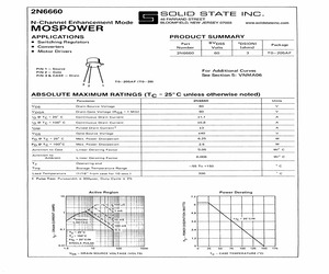
7 Pages, 121 KB, Original2N6660 SOLID STATE INC. S 46 FARRAND STREET N-Channel! Enhancement Mode BLOOMFIELD, NEW JERSEY 07003 MOSPOWER www.solidstateinc.com a Switching Regulators Part BVpss 'DS(ON) Package = Converters Number Volts (ohms) = Motor Drivers 2N6660 60 3 TO205AF PIN 1 ~ Source 4: PIN2 Gate. For Additional Curves PIN 3 & CASE Drain See Section 5: VNMA06 TO205AF (TO39) 3 2 1 ABSOLUTE MAXIMUM RATINGS (Tc = 25C unless otherwise noted) Parameter 2N6660 Units Vos Drain-Source Voltage 60 Vv VpoGR Drain-Gate Voltage (Rgs = 1 MQ) 60 Vv Ip @Te=25C Continuous Drain Current 11 A Ip @ Tc = 100 C Continuous Drain Current 0.8 A lom Pulsed Drain Current! +3 A Vos Gate-Source Voltage +40 Vv Pp @Tc=25C Max. Power Dissipation 6.25 Ww Pp @ Tc = 100C Max. Power Dissipation 2.5 Ww Junction to Case Linear Derating Factor 0.05 wh C Junction to Ambient Linear Derating Factor 0.006 wir c TJ Operating and 55 To +150 oc - o+ Tstg Storage Temperature Range Lead Temperature (t/16 from case for 10 secs.) 300 ec 1
 5 Pages, 297 KB, Scan
2N6660, 2N6660-2, 2N6660JANTX, 2N6660JANTXV www.vishay.com Vishay Siliconix N-Channel 60 V (D-S) MOSFET FEATURES PRODUCT SUMMARY VDS (V) 60 RDS(on) () at VGS = 10 V 3 Configuration * Military Qualified * * * * * Single TO-205AD (TO-39) BENEFITS * * * * * * S 1 2 Low On-Resistence: 1.3 Low Threshold: 1.7 V Low Input Capacitance: 35 pF Fast Switching Speed: 8 ns Low Input and Output Leakage APPLICATIONS 3 G Guaranteed Reliability Low Offset Voltage Low-Voltage Operation Easily Driven Without Buffer High-Speed Circuits Low Error Voltage * Hi-Rel Systems * Direct Logic-Level Interface: TTL/CMOS * Drivers: Relays, Solenoids, Lamps, Hammers, Displays, Memories, Transistors, etc. * Battery Operated Systems * Solid-State Relays D Top View ORDERING INFORMATION PART DESCRIPTION/DSCC PART NUMBER PACKAGE 2N6660 2N6660-2 2N6660JANTX VISHAY ORDERING PART NUMBER Commercial 2N6660 Commercial, Lead (Pb)-free 2N6660 6 Pages, 119 KB, Original
6 Pages, 119 KB, Original2N6660, 2N6660-2, 2N6660JANTX, 2N6660JANTXV www.vishay.com Vishay Siliconix N-Channel 60 V (D-S) MOSFET FEATURES PRODUCT SUMMARY VDS (V) 60 RDS(on) () at VGS = 10 V 3 Configuration * Military Qualified * * * * * Single TO-205AD (TO-39) BENEFITS * * * * * * S 1 2 Low On-Resistence: 1.3 Low Threshold: 1.7 V Low Input Capacitance: 35 pF Fast Switching Speed: 8 ns Low Input and Output Leakage APPLICATIONS 3 G Guaranteed Reliability Low Offset Voltage Low-Voltage Operation Easily Driven Without Buffer High-Speed Circuits Low Error Voltage * Hi-Rel Systems * Direct Logic-Level Interface: TTL/CMOS * Drivers: Relays, Solenoids, Lamps, Hammers, Displays, Memories, Transistors, etc. * Battery Operated Systems * Solid-State Relays D Top View ORDERING INFORMATION PART DESCRIPTION/DSCC PART NUMBER PACKAGE 2N6660 2N6660-2 2N6660JANTX VISHAY ORDERING PART NUMBER Commercial 2N6660 Commercial, Lead (Pb)-free 2N6660 6 Pages, 127 KB, Original
6 Pages, 127 KB, Original2N6660 N-Channel, Enhancement-Mode, Vertical DMOS FET Features Description * * * * * * * 2N6660 is an enhancement-mode (normally-off) transistor that utilizes a vertical DMOS structure and a wellproven silicon-gate manufacturing process. This combination produces a device with the power-handling capabilities of bipolar transistors, and the high input impedance and positive temperature coefficient inherent in MOS devices. Characteristic of all MOS structures, this device is free from thermal runaway and thermally-induced secondary breakdown. Free from secondary breakdown Low power drive requirement Ease of paralleling Low CISS and fast switching speeds Excellent thermal stability Integral source-drain diode High input impedance and high gain Applications * * * * * * Motor controls Converters Amplifiers Switches Power supply circuits Drivers: relays, hammers, solenoids, lamps, memories, displays, bipolar transistors, etc. Vertical DMOS FETs are ideally suited to a wide range of switchi
 10 Pages, 452 KB, Original
2N6660, 2N6660-2, 2N6660JANTX, 2N6660JANTXV www.vishay.com Vishay Siliconix N-Channel 60 V (D-S) MOSFET FEATURES PRODUCT SUMMARY VDS (V) 60 RDS(on) () at VGS = 10 V 3 Configuration * Military Qualified * * * * * Single TO-205AD (TO-39) BENEFITS * * * * * * S 1 2 Low On-Resistence: 1.3 Low Threshold: 1.7 V Low Input Capacitance: 35 pF Fast Switching Speed: 8 ns Low Input and Output Leakage APPLICATIONS 3 G Guaranteed Reliability Low Offset Voltage Low-Voltage Operation Easily Driven Without Buffer High-Speed Circuits Low Error Voltage * Hi-Rel Systems * Direct Logic-Level Interface: TTL/CMOS * Drivers: Relays, Solenoids, Lamps, Hammers, Displays, Memories, Transistors, etc. * Battery Operated Systems * Solid-State Relays D Top View ORDERING INFORMATION PART DESCRIPTION/DSCC PART NUMBER PACKAGE 2N6660 2N6660-2 2N6660JANTX VISHAY ORDERING PART NUMBER Commercial 2N6660 Commercial, Lead (Pb)-free 2N6660 6 Pages, 128 KB, Original
6 Pages, 128 KB, Originals and found 4 products matching your criteria. Top of Page If you are unable to find a suitable part, please contact us. file:///G|/imaging/BITTING/seme_html/2N3824.php.html [26-Mar-2002 9:38:53 AM] Search Results Part number search for devices beginning "2N6660" Datasheets are downloaded as Acrobat PDF files. Semelab Home Fet Products ID(cont) (A) PD (W) RDSS () CISS (pF) QG (nC) PRODUCT Polarity Package VDSS (V) 2N6660 N-Channel TO39 60V 1.1A 6.25W 3.0 5pF (max) - 2N6660CSM4 N-Channel LCC3 60V 1.1A 6.25W 3.0 5pF (max) - 2N6660CSM4-JQR-B N-Channel LCC3 60V 1.1A 6.25W 3.0 5pF (max) - 2N6660-JQR-B N-Channel TO39 60V 1.1A 6.25W 3.0 5pF (max) - 2N6660LCC4 N-Channel LCC4 60V 1.1A 6.25W 3.0 5pF (max) - 2N6660LCC4-JQR-B N-Channel LCC4 60V 1.1A 6.25W 3.0 5pF (max) - 2N6660Q Quad N-Channel LCC6 60V 1.1A 6.25W 3.0 5pF (max) - 2N6660S N-Channel TO39 60V 1.1A 6.25W 3.0 5pF (max) - 2N6660SMD N
 14 Pages, 98 KB, Original
2N6660, 2N6660-2, 2N6660JANTX, 2N6660JANTXV www.vishay.com Vishay Siliconix N-Channel 60 V (D-S) MOSFET FEATURES PRODUCT SUMMARY VDS (V) 60 RDS(on) () at VGS = 10 V 3 Configuration * Military Qualified * * * * * Single TO-205AD (TO-39) BENEFITS * * * * * * S 1 2 Low On-Resistence: 1.3 Low Threshold: 1.7 V Low Input Capacitance: 35 pF Fast Switching Speed: 8 ns Low Input and Output Leakage APPLICATIONS 3 G Guaranteed Reliability Low Offset Voltage Low-Voltage Operation Easily Driven Without Buffer High-Speed Circuits Low Error Voltage * Hi-Rel Systems * Direct Logic-Level Interface: TTL/CMOS * Drivers: Relays, Solenoids, Lamps, Hammers, Displays, Memories, Transistors, etc. * Battery Operated Systems * Solid-State Relays D Top View ORDERING INFORMATION PART DESCRIPTION/DSCC PART NUMBER PACKAGE 2N6660 2N6660-2 2N6660JANTX VISHAY ORDERING PART NUMBER Commercial 2N6660 Commercial, Lead (Pb)-free 2N6660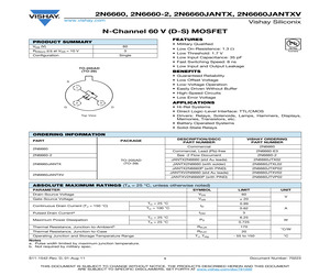 6 Pages, 128 KB, Original
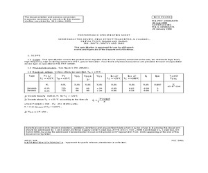
6 Pages, 128 KB, Originalcomply with this revision shall be completed by 30 October 1999 INCH-POUND MIL-PRF-19500/547B 30 July 1999 SUPERSEDING MIL-S-19500/547A 20 January 1988 PERFORMANCE SPECIFICATION SHEET SEMICONDUCTOR DEVICE, FIELD EFFECT TRANSISTOR, N-CHANNEL, SILICON TYPES 2N6660 AND 2N6661 JAN, JANTX, JANTXV AND JANS This specification is approved for use by all Departments and Agencies of the Department of Defense. 1. SCOPE 1.1 Scope. This specification covers the performance requirements for a N-channel, enhancement-mode, low-threshold logic level, high frequency, high switching speed MOSFET, power transistor. Four levels of product assurance are provided for each encapsulated device type as specified in MIL-PRF-19500. 1.2 Physical dimensions. See figure 1 (TO-205AD). 1.3 Maximum ratings. Unless otherwise specified, TA = +25C. Type 2N6660 2N6661 PT 1/ PT TC = +25C TA = +25C VDS VDGR VGS 3/ ID1 2/ ID2 2/ TC = +25C TC = +100C IS IDM TJ and TSTG C -65 to +150 W mW V dc V dc V dc A dc A dc A dc A(pk) 6
 17 Pages, 74 KB, Original
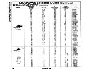
40 6.0 0.8 6.25 VN2406B 170 6.0 0.8 6.25 VN1706B 120 6.0 0.8 6.25 VN1206B 100 0.3 6.0 20 IRFF120 100 0.4 5.0 20 IRFF122 90 4.0 0.9 6.25 2N6661 90 45 0.9 6.25 VNI9SAB 90 5.0 0.8 6.25 VNS0AB 60 0.3 6.0 20 IRFF121 + 60 0.4 5.0 20 IRFF123 0-38 60 3.0 1.1 6.25 2N6660 60 3.5 1.0 6.25 VN67AB 35 1.8 1.4 6.25 2N6659 _35 25 412 6.25 VN35AB Siliconix2N6660 = VN6/AB MOSPOWER FEATURES High Input Impedance a Extremely Fast Switching ms Rugged Dissipation Limited SOA a Internal Drain-Source Diode BENEFITS a Reduced Component Count a Simpler Designs Directly Interfaces CMOS & TTL = Improved Circuit Performance a Increased Reliability N-Channel Enhancement Mode ss Siliconix These power FETs are designed especially for low power high frequency inverters, interface to CMOS and TTL logic, and line drivers. Product Summary BVoss Ropsion) Part Number (Volts) (Ohms) Package 2N6660 | 60 3 TO-39 VN67AB 60 3.5 TO-39 a 8 Drain-Source Voltage .............. 60V Drain-Gate Voltage ................ 6
 6 Pages, 215 KB, Scan
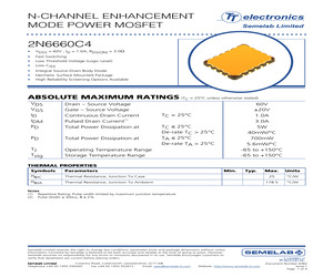
2N6660C4 * VDSS = 60V , ID = 1.0A, RDS(ON) = 3.0 * * * Fast Switching Low Threshold Voltage (Logic Level) Low CISS * * * Integral Source-Drain Body Diode Hermetic Surface Mounted Package High Reliability Screening Options Available ABSOLUTE MAXIMUM RATINGS (TC = 25C unless otherwise stated) VDS VGS ID IDM PD Drain - Source Voltage Gate - Source Voltage Continuous Drain Current (1) Pulsed Drain Current Total Power Dissipation at PD Total Power Dissipation at TJ Tstg Operating Temperature Range Storage Temperature Range 60V 20V 1.0A 3.0A 5W 40mW/C 700mW 5.6mW/C -65 to +150C -65 to +150C TC = 25C TC 25C De-rate TC > 25C TA 25C De-rate TA > 25C THERMAL PROPERTIES Symbols Parameters RJC Thermal Resistance, Junction To Case RJA Thermal Resistance, Junction To Ambient Min. Typ. Max. Units 25 C/W 178.5 C/W Notes (1) Repetitive Rating: Pulse width limited by maximum junction temperature (2) Pulse Width 300us, 2% Semelab Limited reserves the right to change test conditions, parameter limits and package dim
 4 Pages, 236 KB, Original
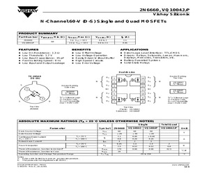
2N6660, VQ1004J/P Vishay Siliconix N-Channel 60-V (D-S) Single and Quad MOSFETs PRODUCT SUMMARY Part Number V(BR)DSS Min (V) 2N6660 rDS(on) Max (W) 60 VQ1004J/P VGS(th) (V) ID (A) 3 @ VGS = 10 V 0.8 to 2 1.1 3.5 @ VGS = 10 V 0.8 to 2.5 0.46 FEATURES BENEFITS APPLICATIONS D D D D D D D D D D D Direct Logic-Level Interface: TTL/CMOS D Drivers: Relays, Solenoids, Lamps, Hammers, Displays, Memories, Transistors, etc. D Battery Operated Systems D Solid-State Relays Low On-Resistance: 1.3 W Low Threshold: 1.7 V Low Input Capacitance: 35 pF Fast Switching Speed: 8 ns Low Input and Output Leakage Low Offset Voltage Low-Voltage Operation Easily Driven Without Buffer High-Speed Circuits Low Error Voltage Dual-In-Line TO-205AD (TO-39) N S D1 1 14 D4 S1 2 13 S4 3 12 G4 4 11 G1 Device Marking Side View 1 NC 2N6660 "S" fllxxyy 2 3 G D "S" = Siliconix Logo f = Factory Code ll = Lot Traceability xxyy = Date Code 5 10 G3 S2 6 9 S3 D2 7 8 D3 Top View 2N6660 N VQ1004J "S" fllx
 5 Pages, 80 KB, Original
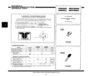
igh-speed switching appli- N-CHANNEL TMOS cations such as switching power supplies, CMOS logic. micropro- FET cessor or TTL-to-high current interface and line drivers 60, 90 VOLTS Fast Switching Speed ton = tof = 5.0 ns Max @ Low On-Resistance 2.0 Ohm Typ 2N6660/2N6661 i} MPF6660/MPF6661 Low Drive Requirement, Vgsith) = 2.0 V Max @ Inherent Current Sharing Capability Permits Easy Paraileling of Many Devices 2N6660 2N6661 0 G TMOS $ CASE 79-04 TO-205AD MAXIMUM RATINGS 2N6660 2N6661 Rating Symbol MPF6660 MPF6661 Unit Drain-Source Voltage Vpss 60 90 Vde Drain-Gate Voltage VoGo 60 90 Vde Gate-Source Voltage V6s + 30 Vde Drain Current MPF6660 Continuous (1) Ip 2.0 Ade Pulsed (2) IDM 3.0 THERMAL CHARACTERISTICS Total Power Dissipation Pp @ Tc = 25C 6.25 2.5 Watts Derate above 25C 50 20 mwrc Total Power Dissipation Pp fa Ta = 26C _ 1.0 Watts Derate above 25C 8.0 mWw.C Operating and Storage TJ. Tstg 55 to +150 c Temperature Range (1) The Power Dissipation of the package may resu
 4 Pages, 107 KB, Scan
2N6660, VQ1004J/P Vishay Siliconix N-Channel 60-V (D-S) Single and Quad MOSFETs PRODUCT SUMMARY Part Number V(BR)DSS Min (V) 2N6660 rDS(on) Max (W) 60 VQ1004J/P VGS(th) (V) ID (A) 3 @ VGS = 10 V 0.8 to 2 1.1 3.5 @ VGS = 10 V 0.8 to 2.5 0.46 FEATURES BENEFITS APPLICATIONS D D D D D D D D D D D Direct Logic-Level Interface: TTL/CMOS D Drivers: Relays, Solenoids, Lamps, Hammers, Displays, Memories, Transistors, etc. D Battery Operated Systems D Solid-State Relays Low On-Resistance: 1.3 W Low Threshold: 1.7 V Low Input Capacitance: 35 pF Fast Switching Speed: 8 ns Low Input and Output Leakage Low Offset Voltage Low-Voltage Operation Easily Driven Without Buffer High-Speed Circuits Low Error Voltage Dual-In-Line TO-205AD (TO-39) N S D1 1 14 D4 S1 2 13 S4 3 12 G4 4 11 G1 Device Marking Side View 1 NC 2N6660 "S" fllxxyy 2 3 G D "S" = Siliconix Logo f = Factory Code ll = Lot Traceability xxyy = Date Code 5 10 G3 S2 6 9 S3 D2 7 8 D3 Top View 2N6660 N VQ1004J "S" fllx
 4 Pages, 51 KB, Original


