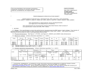
ary to comply with this revision shall be completed by 30 August 2008 * INCH-POUND MIL-PRF-19500/461F 30 May 2008 SUPERSEDING MIL-PRF-19500/461E 18 April 2003 PERFORMANCE SPECIFICATION SHEET SEMICONDUCTOR DEVICE, TRANSISTOR, PNP, SILICON, HIGH-POWER, TYPE 2N6211, 2N6212, 2N6213, 2N6213A, JAN, JANTX, JANTXV, JANS, JANHC, AND JANKC This specification is approved for use by all Departments and Agencies of the Department of Defense. * The requirements for acquiring the product described herein shall consist of this specification sheet and MIL-PRF-19500. 1. SCOPE 1.1 Scope. This specification covers the performance requirements for PNP silicon, high-voltage. Four levels of product assurance are provided for each device type as specified in MIL-PRF-19500. Two levels of product assurance are provided for each unencapsulated device type. 1.2 Physical dimensions. See figure 1 (TO-66), and figure 2, JANHC and JANKC (die) dimensions. 1.3 Maximum ratings. Unless otherwise specified, TC = +25C. Type 2N6
 17 Pages, 195 KB, Original
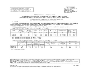
n measures necessary to comply with this revision shall be completed by 14 September 2001. MIL-PRF-19500/461D 14 June 2001 SUPERSEDING MIL-PRF-19500/461C 29 May 1998 PERFORMANCE SPECIFICATION SEMICONDUCTOR DEVICE, TRANSISTOR, PNP, SILICON, HIGH-POWER TYPE 2N6211, 2N6212, 2N6213, JAN, JANTX, JANTXV, JANS, JANHC, AND JANKC This specification is approved for use by all Departments and Agencies of the Department of Defense. 1. SCOPE 1.1 Scope. This specification covers the performance requirements for PNP silicon, high-voltage. Four levels of product assurance are provided for each device type as specified in MIL-PRF-19500. Two levels of product assurance are provided for each unencapsulated device type. 1.2 Physical dimensions. See figure 1 (TO-66), and figure 2, JANHC and JANKC (die) dimensions. 1.3 Maximum ratings. Unless otherwise specified, TC = +25C. Type 2N6211 2N6212 2N6213 (1) (2) PT (1) TA = +25C W PT (2) TC = +25C W VCBO VCEO VEBO IB IC TOP and TSTG RJC (max) ZJX V dc V dc V d
 19 Pages, 113 KB, Original
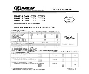
2N6211 JAN, JTX, JTXV 2N6212 JAN, JTX, JTXV 2N6213 JAN, JTX, JTXV MIL-PRF QPL DEVICES Processed per MIL-PRF-19500/461 PNP HIGH-POWER SILICON TRANSISTOR MAXIMUM RATINGS Ratings Collector-Emitter Voltage Collector-Base Voltage Emitter-Base Voltage Base Current Collector Current Total Power Dissipation @ TA = 250C (1) @ TC = 250C (2) Operating & Storage Junction Temperature Range Symbol 2N6211 2N6212 2N6213 Units VCEO VCBO VEBO IB IC PT 225 275 300 350 6.0 1.0 2.0 350 400 Vdc Vdc Vdc Adc Adc 3.0 35 TJ, Tstg W W 0 -55 to +200 C THERMAL CHARACTERISTICS Characteristics Thermal Resistance Junction-to-Case 1) 2) TO-66 (TO-213AA) Symbol Max. 5.0 RJC Derate linearly 17.1 mW/0C for TA > 250C Derate linearly 200 mW/0C for TC > 250C Unit 0 C/W ELECTRICAL CHARACTERISTICS (TC = 250C unless otherwise noted) Characteristics Symbol Min. Max. Unit 2N6211 2N6212 2N6213 V(BR)CEO 225 300 350 Vdc 2N6211 2N6212 2N6213 V(BR)CER 250 325 375 Vdc OFF CHARACTERISTICS Collector-Emitter B
 2 Pages, 23 KB, Original
N6051UTXV 3-143 2N6192 2N6193 3-158 2N6052 2N6052 3-143 2N6193 2N6193 3-158 2N6052JAN 2N6052JAN 3-143 2N6193JAN 2N6193JAN 3-158 2N6052JTX 2N6052JTX 3-143 2N6193JTX 2N6193JTX 3-158 2N6052JTXV 2N6052JTXV 3-143 2N6193JTXV 2N6193JTXV 3-158 2N6053 2N6053 3-147 2N6211 2N6211 3-161 2N6054 2N6054 3-147 2N6212 2N6212 3-161 2N6055 2N6055 3-147 2N6213 2N6213 3-161 2N6056 2N6056 3-147 2N6226 MJ15016 3-9 2N6057 2N6057 3-143 2N6227 MJ150176 3-9 2N6058 2N6058 3-143 2N6228 MJ15016 39 2N6058JAN 2N6058JAN 3-143 2N6229 2N5880 3-123 2N6058JTX 2NG6058JTX 3-143 2N6230 MJ15002 3-710 2NG058JTXV 2NGO58JTXV 3-143 2N6231 MJ15002 3-710 2N6059 2N6059 3-143 2N6233 2N3584 3-20 2N6059JAN 2N6059JAN 3-143 2N6234 2N3585 3-20 2N6059JTX 2N6059/TX 3-143 2N6235 2N3585 3-20 2N6059JTXV 2N6059JTXV 3-143 2N6242 MJ13015 3-670 2N6077 2N3585 3-20 2N6243 MJ13335 3-700 2N6078 2N3585 3-20 2N6244 MJ13333 3-700 2N6079 2N3585 3-20 2N6245 MJ13335 3-700 2N6098 2N6487 3-207 2N6246 2N5879 3123 2N6099 2N6487 3-207 2N6247 2N5880 3-123 2N610
 6 Pages, 232 KB, Scan
2N6211, 2N6212, 2N6213, 2N6214 High-Voltage Medium-Power Silicon P-N-P Transistors For Switching and Amplifier Applications in Military, Industrial, and Commerical Equipment Features: a High voltage ratings: Vceo(sus) = -400 V max. (2N6214) = -350 V max. (2N6213) = -300 V max. (2N6212) Appilcations: @ Power-Switching circuits Switching regulators Converters Inverters File Number 507 = -225 V max. (2N6211) RCA types 2N6211, 2N6212, 2N6213, and 2N6214 are epitaxial silicon p-n-p transistors with high breakdown- voltage ratings and fast switching speeds. They are supplied in the popular JEDEC TO-213AA package; they differ in breakdown-voitage ratings and leakage current values. Formerly RCA Dev. Nos. TA7719, TA7410, TA8330, and TA8331, respectively. MAXIMUM RATINGS, Absolute-Maximum Values: 2N6211 * COLLECTOR-TO-BASE VOLTAGE, Veno.....-+-0+-00s -275 COLLECTOR-TO-EMITTER SUSTAINING VOLTAGE: With base open, Vceo(SUS) ....-+.seececersenertenens -225 With external
 5 Pages, 363 KB, Scan
al limitations will reduce the power that can be handled to vatues 50 less than the limitations Imposed by second breakdown, (See Vee: COLLECTOR-EMITTER VOLTAGE (VOLTS) Figure 8). 2N621 0.02 0.01 10 3-161 MOTORCLA SC XSTRS/R F L2E D Bf esezesy o084L07 3 i 2N6211, 2N6212, 2N6213 ELECTRICAL CHARACTERISTICS (Tc = 26C unless otherwise noted) 7-33-/9 Characteristic |] Symbo! |] Min Max unit | OFF CHARACTERISTICS *Collector-Emitter Sustaining Voltage (1) Vceoisus) Vde (tg = 200 mAde, Ig 70) 2N6211 225 - 2N6212 300 - 2N6213 350 - *Collector-Emitter Sustaining Voltage VCEX (sus) Vde (Ig = 200 mA, Veg = -1.5 V, L = 10 mH) 2N6211 275 - 2N6212 360 ~ 2N6213 400 - *Collector-Emitter Sustaining Voltage (1) VcER[sus) Vde (Ig = 200 mA, Ig = 0, Age =50 2) 2N6211 260 - 2N6212 325 - 2N6213 375 - *Emitter-Base Breskdown Voltage (1) Vegso Vide (Ig = 0.5 mAdc, Ig = 0) 2N6212/13 6.0 - (ig = 1.0 mAde, Ic = 0} 2N6211 6.0 - Collector Cutoff Current Icev mAdc (Vog = 250 V
 3 Pages, 231 KB, Scan
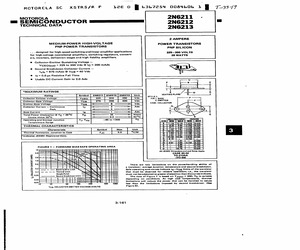
voltage operational amplifier, switching regulators, converters, inverters, deflection stages and hig fidelity amplifiers. FEATURES: * Collector-Emitter Sustaining Voltage- VeEoisus)= 225-350V@I,= 200mA * Usable DC Current Gain to 2.0A MAXIMUM RATINGS PNP 2N6211 2N6212 2N6213 2 AMPERE POWER TRANSISTORS PNP SILICON 225 -350 VOLTS 35 WATTS Characteristic Symbol | 2N6211 | 2N6212 | 2N6213 | Unit Collector-Base Voltage Vopo 275 350 400 Vv Coliector-Emitter Voltage Voeo 225 300 350 Vv Emitter-Base Voltage Veso 6.0 Vv Collector Current - Continuous Ic 2.0 A Peak low 5.0 Base Current-Peak lp 1.0 A Total Power Dissipation @T,= 25C} PP, 35 Ww Derate above 25C 0.2 wre Operating and Storage Junction Ty: Tst c Temperature Range -65 to +200 THERMAL CHARACTERISTICS Characteristic Symbol Max UNIT Thermai Resistance Junction to Case R8jc 5.0 c FIGURE -1 POWER DERATING Pp, POWER DISSIPATIONWATTS) ono aBeRsvss 0 6&6 SN 7 100 T., TEMPERATURE( C) 125 150 175 200 "oz | PIN 1.BASE 2.EMITTER 3.COLLECTOR(CA
 3 Pages, 143 KB, Original
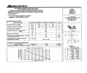
2N6211 2N6212 MAXIMUM RATINGS Ratings Collector-Emitter Voltage Collector-Base Voltage Emitter-Base Voltage Base Current Collector Current Total Power Dissipation JAN JANTX JANTXV 2N6213 Symbol 2N6211 2N6212 2N6213 Unit VCEO VCBO VEBO IB IC @ TA = +250C (1) PT @ TC = +250C (2) Operating & Storage Temperature Top, Tstg 225 275 300 350 350 400 6.0 1.0 2.0 3.0 35 -55 to +200 Vdc Vdc Vdc Adc Adc W W 0 C Characteristics Thermal Resistance Junction-to-Case 1) Derate linearly 17.1 mW/0C for TA > +250C 2) Derate linearly 200 mW/0C for TC > +250C TO-66* (TO-213AA) THERMAL CHARACTERISTICS Symbol RJC Max. 5.0 Unit C/W 0 *See appendix A for package outline ELECTRICAL CHARACTERISTICS (TC = 250C unless otherwise noted) Characteristics Symbol Min. Max. Unit 2N6211 2N6212 2N6213 V(BR)CEO 225 300 350 Vdc 2N6211 2N6212 2N6213 V(BR)CER 250 325 375 Vdc OFF CHARACTERISTICS Collector-Emitter Breakdown Voltage IC = 200 mAdc, f = 30-60 Hz Collector-Emitter Breakdown Voltage IC = 20
 2 Pages, 47 KB, Original
N6051UTXV 3-143 2N6192 2N6193 3-158 2N6052 2N6052 3-143 2N6193 2N6193 3-158 2N6052JAN 2N6052JAN 3-143 2N6193JAN 2N6193JAN 3-158 2N6052JTX 2N6052JTX 3-143 2N6193JTX 2N6193JTX 3-158 2N6052JTXV 2N6052JTXV 3-143 2N6193JTXV 2N6193JTXV 3-158 2N6053 2N6053 3-147 2N6211 2N6211 3-161 2N6054 2N6054 3-147 2N6212 2N6212 3-161 2N6055 2N6055 3-147 2N6213 2N6213 3-161 2N6056 2N6056 3-147 2N6226 MJ15016 3-9 2N6057 2N6057 3-143 2N6227 MJ150176 3-9 2N6058 2N6058 3-143 2N6228 MJ15016 39 2N6058JAN 2N6058JAN 3-143 2N6229 2N5880 3-123 2N6058JTX 2NG6058JTX 3-143 2N6230 MJ15002 3-710 2NG058JTXV 2NGO58JTXV 3-143 2N6231 MJ15002 3-710 2N6059 2N6059 3-143 2N6233 2N3584 3-20 2N6059JAN 2N6059JAN 3-143 2N6234 2N3585 3-20 2N6059JTX 2N6059/TX 3-143 2N6235 2N3585 3-20 2N6059JTXV 2N6059JTXV 3-143 2N6242 MJ13015 3-670 2N6077 2N3585 3-20 2N6243 MJ13335 3-700 2N6078 2N3585 3-20 2N6244 MJ13333 3-700 2N6079 2N3585 3-20 2N6245 MJ13335 3-700 2N6098 2N6487 3-207 2N6246 2N5879 3123 2N6099 2N6487 3-207 2N6247 2N5880 3-123 2N610
 6 Pages, 247 KB, Scan
2N6211 2N6212 MAXIMUM RATINGS Ratings Collector-Emitter Voltage Collector-Base Voltage Emitter-Base Voltage Base Current Collector Current Total Power Dissipation JAN JANTX JANTXV 2N6213 Symbol 2N6211 2N6212 2N6213 Unit VCEO VCBO VEBO IB IC @ TA = +250C (1) PT @ TC = +250C (2) Operating & Storage Temperature Top, Tstg 225 275 300 350 350 400 6.0 1.0 2.0 3.0 35 -55 to +200 Vdc Vdc Vdc Adc Adc W W 0 C Characteristics Thermal Resistance Junction-to-Case 1) Derate linearly 17.1 mW/0C for TA > +250C 2) Derate linearly 200 mW/0C for TC > +250C TO-66* (TO-213AA) THERMAL CHARACTERISTICS Symbol RJC Max. 5.0 Unit C/W 0 *See appendix A for package outline ELECTRICAL CHARACTERISTICS (TC = 250C unless otherwise noted) Characteristics Symbol Min. Max. Unit 2N6211 2N6212 2N6213 V(BR)CEO 225 300 350 Vdc 2N6211 2N6212 2N6213 V(BR)CER 250 325 375 Vdc OFF CHARACTERISTICS Collector-Emitter Breakdown Voltage IC = 200 mAdc, f = 30-60 Hz Collector-Emitter Breakdown Voltage IC = 20
 3 Pages, 49 KB, Original
2N6211 JAN, JTX, JTXV 2N6212 JAN, JTX, JTXV 2N6213 JAN, JTX, JTXV Processed per MIL-PRF-19500/461 PNP HIGH-POWER SILICON TRANSISTOR MAXIMUM RATINGS Ratings Collector-Emitter Voltage Collector-Base Voltage Emitter-Base Voltage Base Current Collector Current Total Power Dissipation @ TA = 250C (1) @ TC = 250C (2) Operating & Storage Junction Temperature Range Symbol 2N6211 2N6212 2N6213 Units VCEO VCBO VEBO IB IC PT 225 275 300 350 6.0 1.0 2.0 350 400 Vdc Vdc Vdc Adc Adc 3.0 35 TJ, Tstg W W 0 -55 to +200 C THERMAL CHARACTERISTICS Characteristics Thermal Resistance Junction-to-Case 1) 2) TO-66 (TO-213AA) Symbol Max. 5.0 RJC Derate linearly 17.1 mW/0C for TA > 250C Derate linearly 200 mW/0C for TC > 250C Unit 0 C/W ELECTRICAL CHARACTERISTICS (TC = 250C unless otherwise noted) Characteristics Symbol Min. Max. Unit 2N6211 2N6212 2N6213 V(BR)CEO 225 300 350 Vdc 2N6211 2N6212 2N6213 V(BR)CER 250 325 375 Vdc OFF CHARACTERISTICS Collector-Emitter Breakdown Voltage IC
 2 Pages, 64 KB, Original
2N6211, 2N6212, 2N6213, 2N6214 SbE D MM 4302271 0040515 T3b MBHAS 1733-19 For Switching and Amplifier Applications in Military, Industrial, and Commerical Equipment Features: High voltage ratings: Vceo(sus) = -400 V max. (2N6214) a = -350 V max. (2N6213) s = -300 V max. (2N6212) = -225 V max. (2N6211) Applications: Power-Switching circuits Switching regulators Converters Inverters High-Fidelity amplifiers TERMINAL DESIGNATIONS The types 2N6211, 2N6212, 2N6213, and 2N6214 are epitaxial silicon p-n-p transistors with high breakdown voltage ratings and fast switching speeds. They are supplied EN in the popular JEDEC TO-213AA package; they differ in breakdown-voltage ratings and leakage current values. *Formerly RCA Dev. Nos. TA7719, TA7410, TA8930, and TA8331, respectively. MAXIMUM RATINGS, Absolute-Maximum Values: * COLLECTOR-TO-BASE VOLTAGE, Veno.............. COLLECTOR-TO-EMITTER SUSTAINING VOLTAGE: With base open, Voeo(SuS) ...............ce cee e eee ee With external b
 5 Pages, 325 KB, Scan
2N6211, 2N6212, 2N6213, 2N6214 High-Voltage Medium-Power Silicon P-N-P Transistors For Switching and Amplifier Applications in Military, Industrial, and Commerical Equipment Features: Applications: a High voltage ratings: = Power-Switching circuits Veeo(sus) = -400 V max. (2N6214) Switching regulators = -350 V max. (2N6273) = Converters = -300 V max. (2N6212) a Inverters = -225 V max. (2N6271) 8 High-Fidelity amplifiers TERMINAL DESIGNATIONS The types 2N6211, 2N6212, 2N6213, and 2N6214 are epitaxial silicon p-n-p transistors with high breakdown voltage ratings and fast switching speeds. They are supplied EN in the popular JEDEC TO-213AA package; they differ in breakdown-voitage ratings and leakage current values. c {FLANGE} *Formerty RCA Dev. Nos. TA7719, TA7410, TA8330, and TA8331, respectively. POWER TRANSISTORS 92CS-27516 JEDEC TO-213AA MAXIMUM RATINGS, Abso/ute-Maximum Values: 2N6211 2N6212 2N6213 2N6214 * COLLECTOR-TO-BASE VOLTAGE, Veao.........-.... 275 -350 -400 -
 5 Pages, 217 KB, Scan
2N6211, 2N6212, 2N6213, 2N6214 High-Voltage Medium-Power Silicon P-N-P Transistors For Switching and Amplifier Applications in Military, Industrial, and Commerical Equipment Features: a High voltage ratings: s Vceo(sus) = -400 V max. (2N6214) = -350 V max. (2N6213) = -300 V max. (2N6212) = -225 V max. (2N6271) Applications: Power-Switching circuits Switching regulators Converters Inverters High-Fidelity amplifiers RCA types 2N6211, 2N6212, 2N6213, and 2N6214 are epitaxial silicon p-n-p transistors with high breakdown- voltage ratings and fast switching speeds. They are supplied in the popular JEDEC TO-213AA package; they differ in breakdown-voitage ratings and leakage current values. Formerly RCA Dev. Nos. TA7719, TA7410, TA8330, and TA8331, respectively. MAXIMUM RATINGS, Absolute-Maximum Values: * COLLECTOR-TO-BASE VOLTAGE, Veno.....++eeessee COLLECTOR-TO-EMITTER SUSTAINING VOLTAGE: With base open, Veeo(SUS) .......eecceerr ener teeoes With external base-to-emitter resistance (Roe)
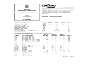
 5 Pages, 238 KB, Scan
2N6211 2N6212 2N6213 SILICON NPN POWER TRANSISTORS w w w. c e n t r a l s e m i . c o m DESCRIPTION: The CENTRAL SEMICONDUCTOR 2N6211, 2N6212, and 2N6213 are silicon NPN transistors designed for high speed switching and high voltage amplifier applications. MARKING: FULL PART NUMBER TO-66 CASE MAXIMUM RATINGS: (TC=25C) Collector-Base Voltage Collector-Emitter Voltage Emitter-Base Voltage Continuous Collector Current Peak Collector Current Continuous Base Current Power Dissipation Operating and Storage Junction Temperature Thermal Resistance SYMBOL VCBO VCEO VEBO IC ICM IB PD TJ, Tstg JC 2N6211 275 225 2N6212 350 300 6.0 2.0 5.0 1.0 35 -65 to +200 5.0 ELECTRICAL CHARACTERISTICS: (TC=25C unless otherwise noted) 2N6211 2N6212 SYMBOL TEST CONDITIONS MIN MAX MIN MAX ICEV VCE=250V, VBE=1.5V 0.5 ICEV VCE=315V, VBE=1.5V 0.5 ICEV VCE=360V, VBE=1.5V ICEV VCE=250V, VBE=1.5V, TC=100C 5.0 ICEV VCE=315V, VBE=1.5V, TC=100C 5.0 ICEV VCE=360V, VBE=1.5V, TC=100C ICEO VCE=150V
 2 Pages, 489 KB, Original


