2N3700J) * JANTX level (2N3700JX) * JANTXV level (2N3700JV) * JANS level (2N3700JS) * JANSR level (2N3700JSR) * QCI to the applicable level * 100% die visual inspection per MIL-STD-750 method 2072 for JANTXV and JANS * Radiation testing (total dose) upon request Features * * * * Hermetically sealed TO-18 metal can Also available in chip configuration Chip geometry 4500 Reference document: MIL-PRF-19500/391 Benefits * Qualification Levels: JAN, JANTX, JANTXV, JANS and JANSR * Radiation testing available Please contact SEMICOA for special configurations www.SEMICOA.com or (714) 979-1900 Absolute Maximum Ratings Parameter Collector-Emitter Voltage Collector-Base Voltage Emitter-Base Voltage Collector Current, Continuous Power Dissipation, TA = 25OC Derate linearly above 37.5OC Power Dissipation, TC = 25OC Derate linearly above 25OC Thermal Resistance Operating Junction Temperature Storage Temperature Copyright 2010 Rev. F TC = 25C unless otherwise
 2 Pages, 433 KB, Original
2N3700J) * JANTX level (2N3700JX) * JANTXV level (2N3700JV) * JANS level (2N3700JS) * QCI to the applicable level * 100% die visual inspection per MIL-STD-750 method 2072 for JANTXV and JANS * Radiation testing (total dose) upon request Features * * * * Hermetically sealed TO-18 metal can Also available in chip configuration Chip geometry 4500 Reference document: MIL-PRF-19500/391 Benefits * Qualification Levels: JAN, JANTX, JANTXV and JANS * Radiation testing available Please contact Semicoa for special configurations www.SEMICOA.com or (714) 979-1900 Absolute Maximum Ratings Parameter Collector-Emitter Voltage Collector-Base Voltage Emitter-Base Voltage Collector Current, Continuous Power Dissipation, TA = 25OC Derate linearly above 37.5OC Power Dissipation, TC = 25OC Derate linearly above 25OC Thermal Resistance Operating Junction Temperature Storage Temperature Copyright 2002 Rev. F TC = 25C unless otherwise specified Symbol VCEO VCBO VEBO IC PT PT RJA T
 2 Pages, 211 KB, Original
2N3700J) * JANTX level (2N3700JX) * JANTXV level (2N3700JV) * JANS level (2N3700JS) * QCI to the applicable level * 100% die visual inspection per MIL-STD-750 method 2072 for JANTXV and JANS * Radiation testing (total dose) upon request Features * * * * Hermetically sealed TO-18 metal can Also available in chip configuration Chip geometry 4500 Reference document: MIL-PRF-19500/391 Benefits * Qualification Levels: JAN, JANTX, JANTXV and JANS * Radiation testing available Please contact Semicoa for special configurations www.SEMICOA.com or (714) 979-1900 Absolute Maximum Ratings Parameter Collector-Emitter Voltage Collector-Base Voltage Emitter-Base Voltage Collector Current, Continuous Power Dissipation, TA = 25OC Derate linearly above 37.5OC Power Dissipation, TC = 25OC Derate linearly above 25OC Thermal Resistance Operating Junction Temperature Storage Temperature Copyright 2010 Rev. F TC = 25C unless otherwise specified Symbol VCEO VCBO VEBO IC PT PT RJA T
 2 Pages, 287 KB, Original
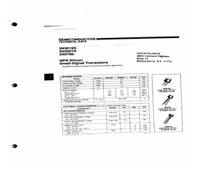
e ViBRICBO (Ig = 100 pAde) Collector Cutot Current (VCE = 90 Vde) (VcE = 90 Vac. Ta = 150 C1 2N3057A CASE 26-03, STYLE 1 Emutter Cutoff Current . Wge = 50 Vdc) TO-206AB (TO-46) 1, Pu'sen Puce Wide 28 2 ers Day Gyre Sot at contin eds2N3019SJAN, 2N3057AJAN, 2N3700JAN SERIES ELECTRICAL CHARACTERISTICS continued Tc = 25C unless otherwise noted.) Characteristic | sympot [owin | Max [unit ON CHARACTERISTICS OC Current Gain NRE (VCE = 10 Vde, ic = 150 mAdc)i1) 100 300 (VCE = 10 Ve, Ic = 0.1 mAdc) 50 200 (VCE = 10 Vde. Ig = 10 mAdc) (1) 90 - (VCE = 10 Vode, ic = 500 mAde}!1) 50 200 (VcE = 10 Vde, IG =1.0nmde 15 _ (VCE = 10 Vdc, Io = 150 mAdc. Ta = ~65C)(1) 40 _ Collector-Emitter Saturation Voitage(1) VCE(sat) (Ig = 150 mAdc, Ig = 15 mAdc) = 02 (ic = 500 mAdc, ig = 50 mAdc} = 0.5 Vde Base-Emitter Saturation Voltage! 1) VBE(saty _ ot (Ig = 150 mAdc, ip = 15 mAde) Vde SMALL-SIGNAL CHARACTERISTICS Smaii-Signal Current Gain Nt (VoE = 5.0 Ve, Ig = 1.0 mAds. f= 1.0 kHz} ao 400 (Vce = 10 Vde. Io = 50 mAdc, f = 2
 2 Pages, 83 KB, Original


