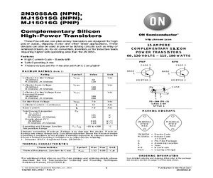
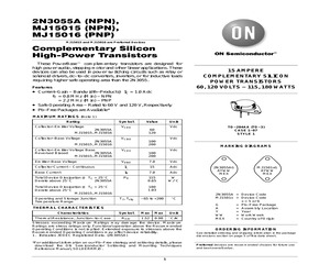
2N3055AG (NPN), MJ15015G (NPN), MJ15016G (PNP) Complementary Silicon High-Power Transistors These PowerBase complementary transistors are designed for high power audio, stepping motor and other linear applications. These devices can also be used in power switching circuits such as relay or solenoid drivers, dc-to-dc converters, inverters, or for inductive loads requiring higher safe operating area than the 2N3055. Features http://onsemi.com 15 AMPERE COMPLEMENTARY SILICON POWER TRANSISTORS 60, 120 VOLTS - 115, 180 WATTS * High Current-Gain - Bandwidth * Safe Operating Area * These Devices are Pb-Free and are RoHS Compliant* PNP Symbol Collector-Emitter Voltage 2N3055AG MJ15015G, MJ15016G VCEO Collector-Base Voltage 2N3055AG MJ15015G, MJ15016G VCBO Collector-Emitter Voltage Base Reversed Biased 2N3055AG MJ15015G, MJ15016G VCEV Emitter-Base Voltage VEBO Value Unit BASE 1 BASE 1 Vdc 60 120 EMITTER 2 EMITTER 2 Vdc CASE 100 200 Vdc 100 200 2 1 7.0 Vdc Collector C
 7 Pages, 136 KB, Original
2N3055AG (NPN), MJ15015G (NPN), MJ15016G (PNP) Complementary Silicon High-Power Transistors These PowerBase complementary transistors are designed for high power audio, stepping motor and other linear applications. These devices can also be used in power switching circuits such as relay or solenoid drivers, dc-to-dc converters, inverters, or for inductive loads requiring higher safe operating area than the 2N3055. Features http://onsemi.com 15 AMPERE COMPLEMENTARY SILICON POWER TRANSISTORS 60, 120 VOLTS - 115, 180 WATTS * High Current-Gain - Bandwidth * Safe Operating Area * These Devices are Pb-Free and are RoHS Compliant* PNP Symbol Collector-Emitter Voltage 2N3055AG MJ15015G, MJ15016G VCEO Collector-Base Voltage 2N3055AG MJ15015G, MJ15016G VCBO Collector-Emitter Voltage Base Reversed Biased 2N3055AG MJ15015G, MJ15016G VCEV Emitter-Base Voltage VEBO Value Unit BASE 1 BASE 1 Vdc 60 120 EMITTER 2 EMITTER 2 Vdc CASE 100 200 Vdc 100 200 2 1 7.0 Vdc Collector C
 6 Pages, 134 KB, Original
2N3055AG (NPN), MJ15015G (NPN), MJ15016G (PNP) Complementary Silicon High-Power Transistors These PowerBase complementary transistors are designed for high power audio, stepping motor and other linear applications. These devices can also be used in power switching circuits such as relay or solenoid drivers, dc-to-dc converters, inverters, or for inductive loads requiring higher safe operating area than the 2N3055. Features http://onsemi.com 15 AMPERE COMPLEMENTARY SILICON POWER TRANSISTORS 60, 120 VOLTS - 115, 180 WATTS * High Current-Gain - Bandwidth * Safe Operating Area * These Devices are Pb-Free and are RoHS Compliant* PNP Symbol Collector-Emitter Voltage 2N3055AG MJ15015G, MJ15016G VCEO Collector-Base Voltage 2N3055AG MJ15015G, MJ15016G VCBO Collector-Emitter Voltage Base Reversed Biased 2N3055AG MJ15015G, MJ15016G VCEV Emitter-Base Voltage VEBO Value Unit BASE 1 BASE 1 Vdc 60 120 EMITTER 2 EMITTER 2 Vdc CASE 100 200 Vdc 100 200 2 1 7.0 Vdc Collector C
 7 Pages, 180 KB, Original
G SC-75 60 MMBT3904LT1G SOT-23 60 MMBT6428LT1G SOT-23 60 MBT3904DW1T1G SOT-363 60 2N3904G TO-92 60 MMBTA05LT1G SOT-23 60 MPSA05RLRAG TO-92 60 MMBT4401LT1G SOT-23 60 2N4401G TO-92 60 2N4922G Case 77 60 TIP31AG TO-220 60 D44H8G TO-220 60 MJE3055TG TO-220 60 2N3055AG TO-3 60 2N3772G TO-3 60 2N5885G TO-3 60 2N5302G TO-3 60 MMBT2484LT1G SOT-23 60 MMBT2222AWT1G SC-70 75 PZT2222AT1G SOT-223 75 MMBT2222ALT1G SOT-23 75 MMBT2222LT1G SOT-23 75 MPS2222AG TO-92 75 PN2222AG TO-92 75 BC846BWT1G SC-70 80 BC846ALT1G SOT-23 80 BC846BLT1G SOT-23 80 MMBT8099LT1G SOT-23 80 MMBTA06LT1G SOT-23 80 MPSA06RLRAG TO-92 80 BCP56-16T1G SOT-223 80 BCP56T1G SOT-223 80 BD139G Case 77 80 2N4923G Case 77 80 MJE182G Case 77 80 mouser.com/onsemi For quantities of 1000 and up, call for quote. IC Max (A) hFE Min 15 5 10 10 4 0.3 0.2 0.6 0.1 0.5 0.5 7 0.5 5 5 0.05 0.1 0.2 0.2 0.2 0.05 0.1 0.2 3 3 4 0.2 0.1 0.1 0.1 0.1 0.1 0.1 0.5 0.5 0.5 0.5 0.2 0.1 0.2 0.2 0.2 0.2 0.2 0.2 0.5 0.5 0.6 0.6 3 3 10 10 15 20 25 30 - 0.6 0.6 0.6 0.6 0.6 0.6
 379 Pages, 47721 KB, Original
J2486 26K5292 42K1300 26K4460 45J1505 1-24 0.60 0.49 0.79 0.32 0.61 0.57 0.55 0.33 0.60 0.30 0.61 0.35 0.79 0.41 0.65 0.42 0.90 0.63 0.61 0.35 0.67 0.35 0.65 0.49 (4250) BIPOLAR POWER TRANSISTORS IN METAL TO-204AA PACKAGE NPN Mfg. Part No. 2N3771G 2N3055G 2N3055AG 2N3772G 2N5886G 2N5038G 2N6284G 2N5302G MJ802G MJ11016G 2N3442G 2N3773G MJ11022G VCEO(sus) Min. (V) 40 60 60 60 80 90 100 100 100 120 140 140 250 IC Max. (A) 30 15 15 20 25 20 20 30 30 30 10 16 15 60 80 100 100 120 120 140 250 200 250 250 15 25 12 20 15 30 20 15 16 16 16 Resistive Switching @ IC tf ts (A) (s) (s) ... ... ... 0.7 Typ. 0.3 Typ. 4 ... ... ... ... ... ... 1 0.8 10 1.5 0.5 12 2.5 Typ. 2.5 Typ. 10 2 1 30 ... ... ... ... ... ... ... ... ... 1.1 Typ. 1.5 Typ. 8 ... ... ... Price Each PD @ 25C (W) 150 115 115 150 200 140 160 200 200 200 117 150 175 Stock No. 26K5275 98H1011 42K3127 26K5276 26K5302 26K5286 26K5315 26K5293 26K4528 26K4505 26K5274 45J2472 42K1311 1-24 3.64 3.20 2.35 2.31 2.85 2.53 4.04 3.89 3.64 3.51 9.00 8.95 4.38
 375 Pages, 58008 KB, Original
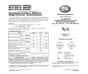
Reversed Biased 2N3055A MJ15015, MJ15016 VCEV Emitter-Base Voltage MARKING DIAGRAMS Vdc 100 200 VEBO 7.0 Vdc Collector Current - Continuous IC 15 Adc Base Current IB 7.0 Adc Total Device Dissipation @ TC = 25_C Derate above 25_C 2N3055A PD 115 0.65 W W/_C 2N3055AG AYWW MEX MJ1501xG AYWW MEX 180 1.03 Total Device Dissipation @ TC = 25_C Derate above 25_C MJ15015, MJ15016 Operating and Storage Junction Temperature Range TO-204AA (TO-3) CASE 1-07 STYLE 1 _C TJ, Tstg -65 to +200 Characteristics Symbol Max Max Unit Thermal Resistance, Junction-to-Case RqJC 1.52 0.98 _C/W THERMAL CHARACTERISTICS 2N3055A = Device Code MJ1501x = Device Code x = 5 or 6 G = Pb-Free Package A = Assembly Location Y = Year WW = Work Week MEX = Country of Origin Stresses exceeding Maximum Ratings may damage the device. Maximum Ratings are stress ratings only. Functional operation above the Recommended Operating Conditions is not implied. Extended exposure to stresses above the Recommended Operating Conditions may affect device
 4 Pages, 73 KB, Original
 40/40 40/-40 45/45 -45/-45 50/-50 0.2/.2 0.2/-0.2 0.1/0.1 -0.1/-0.1 0.1/-0.1 Surface Mount Device For quantities greater than listed, call for quote. hFE Min. 100/100 100/100 200/200 220/220 200/200 ON Semiconductor HIGH-POWER BIPOLAR TRANSISTORS NPN 863-2N3055AG 863-2N3772G 863-2N5885G 863-2N5302G 863-2N5886G 863-MJ802G 863-TIP33CG 863-TIP35CG 863-2N3442G 863-MJE4343G PNP 863-2N5883G 863-2N5884G 863-2N5684G 863-TIP36CG NPN 863-NSS20601CF8T1G 863-NSS40301MZ4T1G 863-NSS60601MZ4T1G PNP 863-NSS12100UW3TCG 863-NSS12100XV6T1G 863-NSS20200LT1G 863-NSS40200LT1G 863-NSS40600CF8T1G NPN 863-MMBT918LT1G 863-MMBT2369ALT1G 863-MMBT2369LT1G 863-MMBTH10LT1G 863-MMBT4401LT1G 863-MMBT4401WT1G PNP 863-MMBT4403LT1G .062 .062 .067 .227 .067 1000 .042 .042 .046 .17 .046 15 20 25 30 25 30 10 25 10 16 10 15 20 15 20 25 20 15 20 15 70 60 100 60 100 100 100 75 70 - 6.15 4.35 3.93 4.15 3.93 3.93 1.69 2.53 6.15 3.34 4.94 3.49 3.15 3.53 3.15 3.15 1.43 2.15 4.94 2.84 4.51 3.18 2.87 3.06 2.87 2.87 1.15 1.72 4.51 2.46 3.06 2.
 1 Pages, 248 KB, Original
Reversed Biased 2N3055A MJ15015, MJ15016 VCEV Emitter-Base Voltage MARKING DIAGRAMS Vdc 100 200 VEBO 7.0 Vdc Collector Current - Continuous IC 15 Adc Base Current IB 7.0 Adc Total Device Dissipation @ TC = 25_C Derate above 25_C 2N3055A PD 115 0.65 W W/_C 2N3055AG AYWW MEX MJ1501xG AYWW MEX 180 1.03 Total Device Dissipation @ TC = 25_C Derate above 25_C MJ15015, MJ15016 Operating and Storage Junction Temperature Range TO-204AA (TO-3) CASE 1-07 STYLE 1 _C TJ, Tstg -65 to +200 Characteristics Symbol Max Max Unit Thermal Resistance, Junction-to-Case RqJC 1.52 0.98 _C/W THERMAL CHARACTERISTICS 2N3055A = Device Code MJ1501x = Device Code x = 5 or 6 G = Pb-Free Package A = Assembly Location Y = Year WW = Work Week MEX = Country of Origin Stresses exceeding Maximum Ratings may damage the device. Maximum Ratings are stress ratings only. Functional operation above the Recommended Operating Conditions is not implied. Extended exposure to stresses above the Recommended Operating Conditions may affect device
 6 Pages, 76 KB, Original


