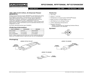
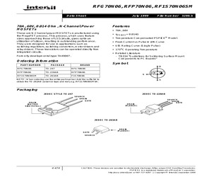
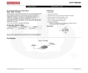
ges that ON Semiconductor was negligent regarding the design or manufacture of the part. ON Semiconductor is an Equal Opportunity/Affirmative Action Employer. This literature is subject to all applicable copyright laws and is not for resale in any manner. RFP70N06 September 2013 Data Sheet Features N-Channel Power MOSFET 60V, 70A, 14 m * 70A, 60V These are N-Channel power MOSFETs manufactured using the MegaFET process. This process, which uses feature sizes approaching those of LSI circuits, gives optimum utilization of silicon, resulting in outstanding performance. They were designed for use in applications such as switching regulators, switching converters, motor drivers and relay drivers. These transistors can be operated directly from integrated circuits. Formerly developmental type TA78440. Ordering Information PART NUMBER RFP70N06 PACKAGE TO-220AB * rDS(on) = 0.014 * Temperature Compensated PSPICE(R) Model * Peak Current vs Pulse Width Curve * UIS Rating Curve (Single Pulse) *
 10 Pages, 697 KB, Original
RFP70N06 September 2013 Data Sheet Features N-Channel Power MOSFET 60V, 70A, 14 m * 70A, 60V These are N-Channel power MOSFETs manufactured using the MegaFET process. This process, which uses feature sizes approaching those of LSI circuits, gives optimum utilization of silicon, resulting in outstanding performance. They were designed for use in applications such as switching regulators, switching converters, motor drivers and relay drivers. These transistors can be operated directly from integrated circuits. Formerly developmental type TA78440. Ordering Information PART NUMBER RFP70N06 PACKAGE TO-220AB * rDS(on) = 0.014 * Temperature Compensated PSPICE(R) Model * Peak Current vs Pulse Width Curve * UIS Rating Curve (Single Pulse) * 175oC Operating Temperature * Related Literature - TB334 "Guidelines for Soldering Surface Mount Components to PC Boards" Symbol BRAND D RFP70N06 G S NOTE: When ordering use the entire part number. Add the suffix 9A to obtain the TO-263AB vari
 8 Pages, 570 KB, Original
RFP70N06, RF1S70N06SM Data Sheet Title FG7 06, P70 6, 1S7 06S bt A, V, 14 m, anwer OSTs) utho eyrds ter- July 1999 70A, 60V, 0.014 Ohm, N-Channel Power MOSFETs Features These are N-Channel power MOSFETs manufactured using the MegaFET process. This process, which uses feature sizes approaching those of LSI circuits, gives optimum utilization of silicon, resulting in outstanding performance. They were designed for use in applications such as switching regulators, switching converters, motor drivers and relay drivers. These transistors can be operated directly from integrated circuits. * rDS(on) = 0.014 Ordering Information PACKAGE TO-247 RFG70N06 RFP70N06 TO-220AB RFP70N06 RF1S70N06SM TO-263AB F1S70N06 * Temperature Compensated PSPICE(R) Model * Peak Current vs Pulse Width Curve * UIS Rating Curve (Single Pulse) * 175oC Operating Temperature * Related Literature - TB334 "Guidelines for Soldering Surface Mount Components to PC Boards" Symbol BRAND RFG70N06 3206.5 * 70A, 60V
 8 Pages, 370 KB, Original
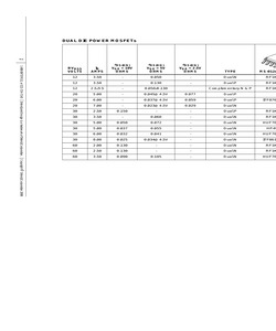
0 - HUF76419P3 - - 60 30.00 - 0.047 - RFP30N06LE - - 60 33.00 0.030 0.035 - HUF76423P3 - - 60 44.00 0.022 0.025 - HUF76429P3 - - 60 45.00 0.028 - - RFP45N06 - - 60 55.00 0.017 0.019 - HUF76432P3 - - 60 64.00 0.014 0.017 - HUF76437P3 - - 60 70.00 0.014 - - RFP70N06 - - 60 70.00 0.014 - RFG70N06 - - - 60 71.00 0.012 0.014 - HUF76439P3 - - 60 75.00 0.0065 0.0075 - HUF76445P3 - - 60 75.00 0.008 0.0095 - HUF76443P3 - - 75 75.00 0.010 - - HUFA7510P3 - - 75 75.00 0.004@12V - HUF75555G3 - - - 80 75.00 0.010 - - HUF75545P3 - - 80 75.00 0.014 - - HUF75542P3 - - 100 1.00 0.600 - - - - IRFD110 MOSFET Selection Guide 1-888-INTERSIL or 321-724-7143 BVDSS VOLTS THRU HOLE N-CHANNEL POWER MOSFETs (Continued) 5 | Copyright (c) Intersil Corporation 2000 ID AMPS rDS(ON) VGS = 10V OHMS rDS(ON) VGS = 5V OHMS TO-247 TO-220AB (I-PAK) TO-251AA (HEXDIP) 4-PIN DIP 100 1.30 0.300 - - - - IRFD120 100 2.00 - 1.050 - RFP2N10L - - 100 5.60 0.540 - - IRF510 - - 100 7.00 - 0.300 - - RFD7N10LE - 100 8.40 0.270 - - - IRFU120 - 100
 2688 Pages, 48746 KB, Original
RFP70N06, RF1S70N06, RF1S70N06SM Data Sheet 70A, 60V, 0.014 Ohm, N-Channel Power MOSFETs These are N-Channel power MOSFETs manufactured using the MegaFET process. This process, which uses feature sizes approaching those of LSI circuits, gives optimum utilization of silicon, resulting in outstanding performance. They were designed for use in applications such as switching regulators, switching converters, motor drivers and relay drivers. These transistors can be operated directly from integrated circuits. Formerly developmental type TA78440. Ordering Information PART NUMBER PACKAGE BRAND RFG70N06 TO-247 RFG70N06 RFP70N06 TO-220AB RFP70N06 RF1S70N06 TO-262AA F1S70N06 RF1S70N06SM TO-263AB F1S70N06 February 2005 Features * 70A, 60V * rDS(on) = 0.014 * Temperature Compensated PSPICE(R) Model * Peak Current vs Pulse Width Curve * UIS Rating Curve (Single Pulse) * 175oC Operating Temperature * Related Literature - TB334 "Guidelines for Soldering Surface Mount Components to PC B
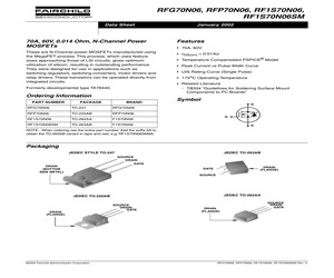
 8 Pages, 196 KB, Original
RFP70N06, RF1S70N06, RF1S70N06SM Data Sheet 70A, 60V, 0.014 Ohm, N-Channel Power MOSFETs These are N-Channel power MOSFETs manufactured using the MegaFET process. This process, which uses feature sizes approaching those of LSI circuits, gives optimum utilization of silicon, resulting in outstanding performance. They were designed for use in applications such as switching regulators, switching converters, motor drivers and relay drivers. These transistors can be operated directly from integrated circuits. Formerly developmental type TA78440. Ordering Information PART NUMBER PACKAGE BRAND RFG70N06 TO-247 RFG70N06 RFP70N06 TO-220AB RFP70N06 RF1S70N06 TO-262AA F1S70N06 RF1S70N06SM TO-263AB F1S70N06 January 2002 Features * 70A, 60V * rDS(on) = 0.014 * Temperature Compensated PSPICE(R) Model * Peak Current vs Pulse Width Curve * UIS Rating Curve (Single Pulse) * 175oC Operating Temperature * Related Literature - TB334 "Guidelines for Soldering Surface Mount Components to PC Bo
 8 Pages, 120 KB, Original
RFP70N06, RF1S70N06SM Data Sheet MAY 2001 70A, 60V, 0.014 Ohm, N-Channel Power MOSFETs [ /Title (RFG7 0N06, RFP70 N06, RF1S7 0N06S /Subject (70A, 60V, 0.014 Ohm, ChanPower MOSFETs) /Autho /Keywords (Inter- * 70A, 60V Formerly developmental type TA78440. Ordering Information PACKAGE TO-247 RFG70N06 RFP70N06 TO-220AB RFP70N06 RF1S70N06SM TO-263AB F1S70N06 * rDS(on) = 0.014 * Temperature Compensated PSPICE(R) Model * Peak Current vs Pulse Width Curve * UIS Rating Curve (Single Pulse) * 175oC Operating Temperature * Related Literature - TB334 "Guidelines for Soldering Surface Mount Components to PC Boards" Symbol BRAND RFG70N06 3206.6 Features These are N-Channel power MOSFETs manufactured using the MegaFET process. This process, which uses feature sizes approaching those of LSI circuits, gives optimum utilization of silicon, resulting in outstanding performance. They were designed for use in applications such as switching regulators, switching converters, motor drivers and
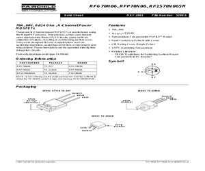 8 Pages, 154 KB, Original
RFP70N06, RF1S70N06SM Data Sheet July 1999 70A, 60V, 0.014 Ohm, N-Channel Power MOSFETs * 70A, 60V Formerly developmental type TA49007. Ordering Information PACKAGE TO-247 RFG70N06 RFP70N06 TO-220AB RFP70N06 RF1S70N06SM TO-263AB F1S70N06 * rDS(on) = 0.014 * Temperature Compensated PSPICE(R) Model * Peak Current vs Pulse Width Curve * UIS Rating Curve (Single Pulse) * 175oC Operating Temperature * Related Literature - TB334 "Guidelines for Soldering Surface Mount Components to PC Boards" Symbol BRAND RFG70N06 3206.5 Features These are N-Channel power MOSFETs manufactured using the MegaFET process. This process, which uses feature sizes approaching those of LSI circuits, gives optimum utilization of silicon, resulting in outstanding performance. They were designed for use in applications such as switching regulators, switching converters, motor drivers and relay drivers. These transistors can be operated directly from integrated circuits. PART NUMBER File Number D G NOTE:
 8 Pages, 72 KB, Original
RFP70N06 September 2013 Data Sheet Features N-Channel Power MOSFET 60V, 70A, 14 m * 70A, 60V These are N-Channel power MOSFETs manufactured using the MegaFET process. This process, which uses feature sizes approaching those of LSI circuits, gives optimum utilization of silicon, resulting in outstanding performance. They were designed for use in applications such as switching regulators, switching converters, motor drivers and relay drivers. These transistors can be operated directly from integrated circuits. Formerly developmental type TA78440. Ordering Information PART NUMBER RFP70N06 PACKAGE TO-220AB * rDS(on) = 0.014 * Temperature Compensated PSPICE(R) Model * Peak Current vs Pulse Width Curve * UIS Rating Curve (Single Pulse) * 175oC Operating Temperature * Related Literature - TB334 "Guidelines for Soldering Surface Mount Components to PC Boards" Symbol BRAND D RFP70N06 G S NOTE: When ordering use the entire part number. Add the suffix 9A to obtain the TO-263AB vari
 9 Pages, 582 KB, Original
RFP70N06, RF1S70N06, RF1S70N06SM S E M I C O N D U C T O R 70A, 60V, Avalanche Rated, N-Channel Enhancement-Mode Power MOSFETs December 1995 Features Packages JEDEC STYLE TO-247 * 70A, 60V SOURCE DRAIN GATE * rDS(on) = 0.014 DRAIN (BOTTOM SIDE METAL) * Temperature Compensated PSPICE Model * Peak Current vs Pulse Width Curve * UIS Rating Curve (Single Pulse) * +175oC Operating Temperature Description The RFG70N06, RFP70N06, RF1S70N06 and RF1S70N06SM are N-channel power MOSFETs manufactured using the MegaFET process. This process, which uses feature sizes approaching those of LSI circuits, gives optimum utilization of silicon, resulting in outstanding performance. They were designed for use in applications such as switching regulators, switching converters, motor drivers and relay drivers. These transistors can be operated directly from integrated circuits. JEDEC TO-220AB SOURCE DRAIN GATE DRAIN (FLANGE) PACKAGE AVAILABILITY PART NUMBER PACKAGE BRAND TO-247 RFG70N06 RFP70N06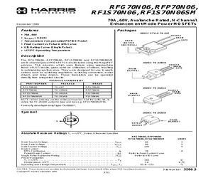 6 Pages, 66 KB, Original
6 Pages, 66 KB, Originalansistor. The switching speed of most PowerMOS transistors is so fast that turn on losses are usually very small. An exception is when the drive current available is very very small. Usually this does not occur in the real world. For example the Fairchild RFP70N06 PowerMOS transistor requires a maximum of 115nC of gate charge to transition from "off" to fully "on". For a gate drive which supplies 1.0mA this would mean that the transition would take less than 115s. This will make a negligible change in the junction temperature of the PowerMOS transistor. Turn-off subjects the PowerMOS transistor to Unclamped Inductive Switching. Modern PowerMOS transistors can withstand this type of stress and give clear ratings in their datasheets to let customers calculate whether or not they are operating within the devices' capability. The energy dissipated in the PowerMOS transistor each time the current is interrupted is: L x I T x V DSS 1- E T = ------------------------------------ x 1 - K x In 1 + -- RL K
 8 Pages, 102 KB, Original
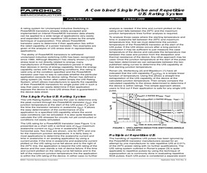
 transistor. The switching speed of most PowerMOS transistors is so fast that turn on losses are usually very small. An exception is when the drive current available is very very small. Usually this does not occur in the real world. For example the Harris RFP70N06 PowerMOS (EQ. 1.1) L L RL + VGS RG + VDD VGS - 0V VDD 0V FIGURE 1. TYPICAL INDUCTIVE SWITCHING CIRCUIT Copyright RG FIGURE 2. SOLENOID SWITCHING APPLICATION CIRCUIT (c) Harris Corporation 1995 1 - Application Note 9512 transistor requires a maximum of 115nC of gate charge to transition from "off" to fully "on". For a gate drive which supplies 1.0mA this would mean that the transition would take less than 115s. This will make a negligible change in the junction temperature of the PowerMOS transistor. A. Try RFP3055 Assume TJ = 175oC. Check to be sure UIS stress is within RFP3055 capability. IT x RL L t AV = ------- x In ------------------------------------------------ + 1 RL 1.3 x V BRK - V CC Turn-off subjects the PowerMOS transistor to
 8 Pages, 42 KB, Original
ransistor. The switching speed of most PowerMOS transistors is so fast that turn on losses are usually very small. An exception is when the drive current available is very very small. Usually this does not occur in the real world. For example the Intersil RFP70N06 PowerMOS transistor requires a maximum of 115nC of gate charge to transition from "off" to fully "on". For a gate drive which supplies 1.0mA this would mean that the transition would take less than 115s. This will make a negligible change in the junction temperature of the PowerMOS transistor. Turn-off subjects the PowerMOS transistor to Unclamped Inductive Switching. Modern PowerMOS transistors can withstand this type of stress and give clear ratings in their datasheets to let customers calculate whether or not they are operating within the devices' capability. The energy dissipated in the PowerMOS transistor each time the current is interrupted is: L x I T x V DSS 1 E T = ------------------------------------ x 1 - K x In 1 + ---- RL K
 8 Pages, 335 KB, Original
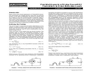
 either case no further (c)2001 Fairchild Semiconductor Corporation IF R = 0 tAV = (L)(lAS)/(1.3 RATED BVDSS - VDD) IF R 0 tAV = (L/R) ln[(IASxR)/(1.3 RATED BVDSS - VDD) + 1] IDN 100 IAS (A) orpoion, minctor, AN-7515 STARTING TJ = 25oC STARTING TJ = 150oC RFP70N06 10 0.01 0.10 1.00 tAV , TIME IN AVALANCHE (ms) 10.00 FIGURE 1. UNCLAMPED-INDUCTIVE-SWITCHING (SINGLE PULSE UIS) Multiple or Repetitive UIS The handling of repetitive UIS pulses has been ignored by the PowerMOS transistor manufacturers except for an attempt by one manufacturer to rate repetitive UIS at 0.01% of the 25oC power rating with no further qualifications. The UIS rating system outlined in Ronan's paper [3] is quite applicable to repetitive pulses by using the technique of superposition as is commonly done in evaluating repetitive SOA pulses. Each UIS pulse is considered a separate event Application Note 7515 Rev. A Application Note 7515 Example 1 DRAIN SOLENOID and evaluated as if no other pulse existed. It is necessary only to
 5 Pages, 311 KB, Original
erMOS transistor users to determine if their application lies within the rated capability of a power transistor. Two examples are given of the analysis of UIS stress level in representative applications. October 1999 STARTING TJ = 25oC STARTING TJ = 150oC RFP70N06 10 0.01 0.10 1.00 tAV, TIME IN AVALANCHE (ms) 10.00 FIGURE 1. UNCLAMPED-INDUCTIVE-SWITCHING (SINGLE PULSE UIS) Multiple or Repetitive UIS The handling of repetitive UIS pulses has been ignored by the PowerMOS transistor manufacturers except for an attempt by one manufacturer to rate repetitive UIS at 0.01% of the 25oC power rating with no further qualifications. The UIS rating system outlined in Ronan's paper [3] is quite applicable to repetitive pulses by using the technique of superposition as is commonly done in evaluating repetitive SOA pulses. Each UIS pulse is considered a separate event Application Note 7515 Rev. A1 Application Note 7515 Example 1 DRAIN SOLENOID and evaluated as if no other pulse existed. It is necessary only to
 5 Pages, 90 KB, Original


