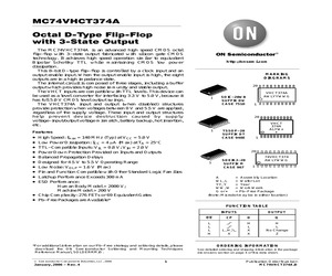
http://onsemi.com 3 Typ Limit TA = - 40 to 85C tw Symbol MC74VHCT374A ORDERING INFORMATION Package Shipping MC74VHCT374ADWR2 SOIC-20WB 1000 / Tape & Reel MC74VHCT374ADWRG SOIC-20WB (Pb-Free) 1000 / Tape & Reel MC74VHCT374ADTR2 TSSOP-20* 2500 / Tape & Reel MC74VHCT374ADTRG TSSOP-20* 2500 / Tape & Reel MC74VHCT374AMEL SOEIAJ-20 2000 / Tape & Reel MC74VHCT374AMELG SOEIAJ-20 (Pb-Free) 2000 / Tape & Reel Device For information on tape and reel specifications, including part orientation and tape sizes, please refer to our Tape and Reel Packaging Specifications Brochure, BRD8011/D. *This package is inherently Pb-Free. 3V 1.5V CP GND tW 1/fmax tPHL tPLH Q VOH 1.5V VOL Figure 3. Switching Waveform 3V OE 1.5V GND tPZL tPLZ tPZH tPHZ HIGH IMPEDANCE 1.5V Q Q VOL +0.3V VOH -0.3V 1.5V HIGH IMPEDANCE Figure 4. Switching Waveform VALID D 3V 1.5V GND th tsu 3V CP 1.5V GND Figure 5. Switching Waveform http://onsemi.com 4 MC74VHCT374A TEST POINT OUTPUT DEVICE UNDER TEST C L* *Includes all probe and jig capacitance
 7 Pages, 109 KB, Original
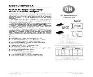
5 2.5 ns th Minimum Hold Time, D to CP VCC = 5.0 0.5 V 2.5 2.5 ns Parameter Test Conditions http://onsemi.com 3 Typ Limit TA = - 40 to 85C tw Symbol MC74VHCT374A ORDERING INFORMATION Package Shipping MC74VHCT374ADWRG SOIC-20WB (Pb-Free) 1000 / Tape & Reel MC74VHCT374ADTRG TSSOP-20 (Pb-Free) 2500 / Tape & Reel Device For information on tape and reel specifications, including part orientation and tape sizes, please refer to our Tape and Reel Packaging Specifications Brochure, BRD8011/D. 3V 1.5V CP GND tW 1/fmax tPHL tPLH VOH Q 1.5V VOL Figure 3. Switching Waveform 3V OE 1.5V GND tPZL tPLZ tPZH tPHZ HIGH IMPEDANCE 1.5V Q VOL +0.3V Q VOH -0.3V 1.5V HIGH IMPEDANCE Figure 4. Switching Waveform VALID 3V D 1.5V GND th tsu 3V CP 1.5V GND Figure 5. Switching Waveform http://onsemi.com 4 MC74VHCT374A TEST POINT OUTPUT DEVICE UNDER TEST CL* *Includes all probe and jig capacitance Figure 6. Test Circuit TEST POINT CONNECT TO VCC WHEN TESTING tPLZ AND tPZL. CONNECT TO GND WHEN TESTING tPHZ AND tPZH. 1 kW OUTPU
 7 Pages, 93 KB, Original
5 2.5 ns th Minimum Hold Time, D to CP VCC = 5.0 0.5 V 2.5 2.5 ns Parameter Test Conditions http://onsemi.com 3 Typ Limit TA = - 40 to 85C tw Symbol MC74VHCT374A ORDERING INFORMATION Package Shipping MC74VHCT374ADWRG SOIC-20WB (Pb-Free) 1000 / Tape & Reel MC74VHCT374ADTRG TSSOP-20* 2500 / Tape & Reel MC74VHCT374AMELG SOEIAJ-20 (Pb-Free) 2000 / Tape & Reel Device For information on tape and reel specifications, including part orientation and tape sizes, please refer to our Tape and Reel Packaging Specifications Brochure, BRD8011/D. *This package is inherently Pb-Free. 3V 1.5V CP GND tW 1/fmax tPLH tPHL VOH Q 1.5V VOL Figure 3. Switching Waveform 3V OE 1.5V GND tPZL tPLZ tPZH tPHZ HIGH IMPEDANCE 1.5V Q VOL +0.3V Q VOH -0.3V 1.5V Figure 4. Switching Waveform HIGH IMPEDANCE VALID 3V D 1.5V GND th tsu 3V CP 1.5V GND Figure 5. Switching Waveform http://onsemi.com 4 MC74VHCT374A TEST POINT OUTPUT DEVICE UNDER TEST CL* *Includes all probe and jig capacitance Figure 6. Test Circuit TEST POINT CONNECT TO V
 8 Pages, 145 KB, Original


