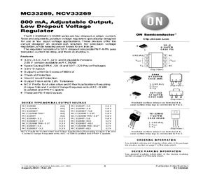
Packages are Available NCV Prefix for Automotive and Other Applications Requiring Site and Control Changes SO-8 D SUFFIX CASE 751 8 Vout Vin 1 8 2 7 3 6 4 5 DPAK DT SUFFIX CASE 369C 1 3 1. GND/Adj 2. Vout 3. Vin 3 SOT-223 ST SUFFIX CASE 318E MC33269D-5.0 MC33269DT-5.0 NCV33269DT-5.0* NCV33269DTRK-5.0* MC33269T-5.0 MC33269D-012 MC33269DT-012 NCV33269DTRK-012* MC33269T-012 1 2 3 (Top View) 1 2 3 Heatsink surface (shown as terminal 4 in case outline drawing) is connected to Pin 2. 5.0 V 5.0 V 5.0 V 5.0 V 5.0 V 12 V 12 V 12 V 12 V *NCV prefix is for automotive and other applications requiring site and change control. NC (Top View) DEVICE TYPE/NOMINAL OUTPUT VOLTAGE Adj Adj Adj Adj 3.3 V 3.3 V 3.3 V 3.3 V 3.3 V Vout (Top View) 1 MC33269D MC33269DT NCV33269DTRK* MC33269T MC33269D-3.3 MC33269DT-3.3 NCV33269DTRK-3.3* MC33269T-3.3 MC33269ST-3.3 NC TO-220AB T SUFFIX CASE 221AB 1 2 3 1. GND/Adj 2. Vout 3. Vin 12 3 (Top View) Heatsink surface (shown as terminal 4 in case outline drawing) is connected to Pin
 13 Pages, 201 KB, Original
w) 1 2 3 (Top View) DEVICE TYPE/NOMINAL OUTPUT VOLTAGE MC33269D NCV33269D* MC33269DT NCV33269DTRK* MC33269T MC33269D-3.3 MC33269DT-3.3 NCV33269DTRK-3.3* MC33269T-3.3 MC33269ST-3.3 Adj Adj Adj Adj Adj 3.3 V 3.3 V 3.3 V 3.3 V 3.3 V MC33269T-3.5 MC33269D-5.0 MC33269DT-5.0 NCV33269DT-5.0* NCV33269DTRK-5.0* MC33269T-5.0 MC33269D-012 MC33269DT-012 NCV33269DTRK-012* MC33269T-012 3.5 V 5.0 V 5.0 V 5.0 V 5.0 V 5.0 V 12 V 12 V 12 V 12 V *NCV Prefix for Automotive and Other Applications Requiring Unique Site and Control Change Requirements; AEC-Q100 Qualified and PPAP Capable. Heatsink surface (shown as terminal 4 in case outline drawing) is connected to Pin 2. TO-220AB T SUFFIX CASE 221AB 1 2 3 1. GND/Adj 2. Vout 3. Vin 12 3 (Top View) Heatsink surface (shown as terminal 4 in case outline drawing) is connected to Pin 2. ORDERING INFORMATION See detailed ordering and shipping information in the package dimensions section on page 7 of this data sheet. DEVICE MARKING INFORMATION See general marking informatio
 13 Pages, 163 KB, Original
45 C49 0.1 uF C5 0.1uF/50V D21 GREEN R40 330 + C48 0.1 uF VCC V_BUS +15V C46 22nF / 400V C1 (1500uF/250V @ 127VAC) (560uF/400V @ 230VAC) B1 1KAB05E-ND S5 470uF/10V + C50 R52 (47K/1W @ 127VAC) (150K/1W @ 230VAC) Figure 3-1. Power Supply - RT1 CL-40 - + IC3 MC33269DT-5.0 3 IN OUT 100nF/25V C19 1 T1 (SW-328 @ 127VAC) (DSW-328 @ 230VAC) 4 2 3 1 2 44 2 DRM007 t EXTERNAL_POWER_SUPPLY_CONNECTOR 1 C47 0.1 uF Freescale Semiconductor, Inc... Freescale Semiconductor, Inc. Schematics and Bill of Materials BLDC Motor Control Board for Industrial and Appliance Applications MOTOROLA C32 0.1uF +15V R39 2.2k C15 0.02uF C14 15pF D20 8.2V S3 ENTER R30 10k VCC FAULT PWM_AT PWM_AB PWM_BT PWM_BB PWM_CT PWM_CB X1 4MHz C13 15pF 1x3 PIN HEADER JP1 VCC C11 0.1uF R23 10k R24 10M R33 VSSA OSC2 OSC1 CGMXFC /IRQ PWM1 PWM2 PWM3 BLDC Motor Control Board for Industrial and Appliance Applications Schematics and Bill of Materials For More Information On This Product, Go to: www.freescale.com R48 100K + VCC R4 1K R60 1K TxD RxD RS
 152 Pages, 1074 KB, Original
GROUND TEST POINT 1 3 EXTERNAL POWER IN INPUT 12V DC P2 1 FM4001 D2 TP5 GROUND TEST POINT 2 1 4 B B +3.3V TP6 1 3 1 U10 D3 VOUT TP7 4 2 4 2 C30 0.1uF C TP8 GROUND TEST POINT FERRITE BEAD L3 FERRITE BEAD L2 M C 33269DT-3.3 GND VOUT FM4001 U11 VIN VOUT VOUT MC33269DT-5.0 GND VIN GROUND TEST POINT +3.3V +5.0V C29 0.1uF 3 FM4001 D1 C +3.3VA Size B L1 C6 4 7 uF 10VDC +3.3V + C5 4 7 uF 10VDC 63A10516S D D Date: Monday, October 16, 2000 Document Number P O W E R SUPPLIES + VCC FERRITE BEAD Title FERRITE BEAD L4 + 5 . 0 V _ U NI3 Figure A-17. Power Supplies +3.3V TEST POINT + C4 470uF 16VDC 1 A 1 56F807EVM Hardware User's Manual For More Information On This Product, Go to: www.freescale.com 1 A-18 3 Freescale Semiconductor, Inc... POWER GOOD LED 2 4 3 Designer: DSPD Design E 18 1.0 Rev. FAX: (480) 413-2510 Sheet 17 of (480) 413-5090 2100 East Elliot Road Tempe, Arizona 85284 DSP Standard Products Division MC33269 1 3.3V AND 5.0V REGULATOR L E D10 GREEN LED R78 470 + 5 .0V E 1 2 3 4 Freescale Semiconducto
 80 Pages, 853 KB, Original
Top View) 1 2 3 (Top View) DEVICE TYPE/NOMINAL OUTPUT VOLTAGE Adj Adj Adj Adj 3.3 V 3.3 V 3.3 V 3.3 V 3.3 V Vout (Top View) 1 MC33269D MC33269DT NCV33269DTRK* MC33269T MC33269D-3.3 MC33269DT-3.3 NCV33269DTRK-3.3* MC33269T-3.3 MC33269ST-3.3 NC MC33269D-5.0 MC33269DT-5.0 MC33269T-5.0 5.0 V 5.0 V 5.0 V Heatsink surface (shown as terminal 4 in case outline drawing) is connected to Pin 2. MC33269D-012 MC33269DT-012 NCV33269DTRK-012* MC33269T-012 12 V 12 V 12 V 12 V TO-220AB T SUFFIX CASE 221AB *NCV prefix is for automotive and other applications requiring site and change control. 1 2 3 1. GND/Adj 2. Vout 3. Vin 12 3 (Top View) Heatsink surface (shown as terminal 4 in case outline drawing) is connected to Pin 2. ORDERING INFORMATION See detailed ordering and shipping information in the package dimensions section on page 7 of this data sheet. DEVICE MARKING INFORMATION See general marking information in the device marking section on page 9 of this data sheet. (c) Semiconductor Components Industries, LLC
 13 Pages, 169 KB, Original
T TARGET INTERFACE AND JTAG CONNECTOR Sheet 16 of E 18 1.0 A-18 A B C D E D1 4 4 FM4001 P2 2 + 5 . 0 V _ U NI3 U10 D2 1 + C4 470uF 16VDC FM4001 3 EXTERNAL POWER IN INPUT 12V DC C29 0.1uF 3 V IN VOUT 2 1 GND VOUT 4 + 5 .0V L1 FERRITE BEAD + C5 4 7 uF 10VDC MC33269DT-5.0 R78 470 POWER GOOD LED DSP56F807EVM Hardware User's Manual L E D10 GREEN LED +5.0V D3 3 3 FM4001 U11 VCC 3 1 V IN GND VOUT 2 VOUT 4 L4 +3.3V FERRITE BEAD M C 33269DT-3.3 + C6 4 7 uF 10VDC L2 +3.3V 2 +3.3VA 3.3V AND 5.0V REGULATOR FERRITE BEAD C30 0.1uF 2 4 L3 FERRITE BEAD 1 2 3 MC33269 TP5 GROUND TEST POINT TP6 DSP Standard Products Division GROUND TEST POINT TP7 2100 East Elliot Road Tempe, Arizona 85284 TP8 1 +3.3V TEST POINT 1 1 TP4 1 TP3 1 GROUND TEST POINT 1 ANALOG GROUND TEST POINT 1 +3.3VA TEST POINT (480) 413-5090 Title +3.3VA +3.3V Size B A B 1 FAX: (480) 413-2510 P O W E R SUPPLIES Document Number Date: Monday, October 16, 2000 C Figure A-17. POWER SUPPLIES Rev. 63A10516S D Designer: DSPD Design Sheet 17 of E 18 1.0 A B C
 80 Pages, 510 KB, Original
Top View) 1 2 3 (Top View) DEVICE TYPE/NOMINAL OUTPUT VOLTAGE Adj Adj Adj Adj 3.3 V 3.3 V 3.3 V 3.3 V 3.3 V Vout (Top View) 1 MC33269D MC33269DT NCV33269DTRK* MC33269T MC33269D-3.3 MC33269DT-3.3 NCV33269DTRK-3.3* MC33269T-3.3 MC33269ST-3.3 NC MC33269D-5.0 MC33269DT-5.0 MC33269T-5.0 5.0 V 5.0 V 5.0 V Heatsink surface (shown as terminal 4 in case outline drawing) is connected to Pin 2. MC33269D-012 MC33269DT-012 NCV33269DTRK-012* MC33269T-012 12 V 12 V 12 V 12 V TO-220AB T SUFFIX CASE 221A *NCV prefix is for automotive and other applications requiring site and change control. 1 2 3 1. GND/Adj 2. Vout 3. Vin 12 3 (Top View) Heatsink surface (shown as terminal 4 in case outline drawing) is connected to Pin 2. ORDERING INFORMATION See detailed ordering and shipping information in the package dimensions section on page 7 of this data sheet. DEVICE MARKING INFORMATION See general marking information in the device marking section on page 9 of this data sheet. (c) Semiconductor Components Industries, LLC,
 13 Pages, 155 KB, Original
Top View) 1 2 3 (Top View) DEVICE TYPE/NOMINAL OUTPUT VOLTAGE Adj Adj Adj Adj 3.3 V 3.3 V 3.3 V 3.3 V 3.3 V Vout (Top View) 1 MC33269D MC33269DT NCV33269DTRK* MC33269T MC33269D-3.3 MC33269DT-3.3 NCV33269DTRK-3.3* MC33269T-3.3 MC33269ST-3.3 NC MC33269D-5.0 MC33269DT-5.0 5.0 V 5.0 V MC33269T-5.0 MC33269D-12 MC33269DT-12 NCV33269DTRK-12* MC33269T-12 5.0 V 12 V 12 V 12 V 12 V *NCV prefix is for automotive and other applications requiring site and change control. Heatsink surface (shown as terminal 4 in case outline drawing) is connected to Pin 2. TO-220AB T SUFFIX CASE 221A 1 2 3 1. GND/Adj 2. Vout 3. Vin 12 3 (Top View) Heatsink surface (shown as terminal 4 in case outline drawing) is connected to Pin 2. ORDERING INFORMATION See detailed ordering and shipping information in the package dimensions section on page 8 of this data sheet. DEVICE MARKING INFORMATION See general marking information in the device marking section on page 10 of this data sheet. (c) Semiconductor Components Industries, LLC, 20
 14 Pages, 156 KB, Original
8 1 Gnd/Adj Vout Vin 1 8 2 7 3 6 4 5 NC DPAK DT SUFFIX CASE 369A 1 Adj Adj Adj 3.3 V 3.3 V 3.3 V 3.3 V Vout (Top View) 3 DEVICE TYPE / NOMINAL OUTPUT VOLTAGE MC33269D MC33269DT MC33269T MC33269D-3.3 MC33269DT-3.3 MC33269T-3.3 MC33269ST-3.3 NC MC33269D-5.0 MC33269DT-5.0 MC33269T-5.0 MC33269D-12 MC33269DT-12 MC33269T-12 5.0 V 5.0 V 5.0 V 12 V 12 V 12 V 1. Gnd/Adj 2. Vout 1 2 3 3. Vin SOT-223 ST SUFFIX CASE 318E (Top View) 1 3 Heatsink surface (shown as terminal 4 in case outline drawing) is connected to Pin 2. TO-220AB T SUFFIX CASE 221A 1 Pin: 1. 2. 3. 2 3 Gnd/Adj Vout Vin 1 2 3 (Top View) Heatsink surface (shown as terminal 4 in case outline drawing) is connected to Pin 2. ORDERING INFORMATION See detailed ordering and shipping information in the package dimensions section on page 7 of this data sheet. Semiconductor Components Industries, LLC, 2000 April, 2000 - Rev. 8 1 Publication Order Number: MC33269/D MC33269 MAXIMUM RATINGS Rating Power Supply Input Voltage Power Dissipation Case 369A (DPAK
 16 Pages, 145 KB, Original
2G MC14536BDWR2G MC14538BDR2G MC14538BDWR2G MC1455BDR2G MC14572UBDR2G MC14584BDG MC1489DG MC33025DWR2G MC3303DR2G MC33079DR2G MC33151PG MC33161PG MC33163DWG MC33166TG MC33167TG MC33171DR2G MC33172PG MC33172VDR2G MC33174DG MC33204DG MC33232DG MC33269D-3.3G MC33269DT-5.0G MC33269T-5.0G MC33272ADG MC33272APG MC33275DT-5.0RKG MC33275ST-5.0T3G MC33340DG MC33340DR2G MC33340PG MC33364DR2G MC33368DR2G MC33368PG MC33375ST-3.3T3G MC33502DR2G MC33503SNT1G MC34025DWR2G MC34025PG MC34064D-005G MC34064D-5R2G MC34064P-5G MC34064P-5RPG MC34072ADG MC34152DG MC34152DR2G MC34164D-3R2G MC34164P-5G MC34166TVG MC44608P40G MC74ACT00DR2G MC74ACT02DR2G MC74ACT08DR2G MC74ACT11DR2G MC74ACT125DR2G MC74ACT14DR2G MC74ACT273DWR2G MC74ACT32DR2G MC74ACT541DWR2G MC74ACT573DWR2G MC74ACT574DWG MC74ACT74DR2G MC74AC00DG MC74AC00DR2G MC74AC125DG MC74AC14DR2G MC74AC257DR2G MC74HCT14ADR2G MC74HCT14ANG MC74HCT245ADWG MC74HCT541ADWR2G MC74HCT74ADR2G MC74HC02ADG MC74HC08ADG MC74HC1G00DTT1G MC74HC1G02DTT1G MC74HC125ADG MC74HC125ADR2G MC74HC
 296 Pages, 947 KB, Original
 For More Information On This Product, Go to: www.freescale.com A B C D 5 5 + 3 .3V FERRITE BEAD L4 FERRITE BEAD L2 P1 2 1 C35 0.1uF FM4001 D2 4 1 1 + 5 .0V 1 + 3 .3V + 3 .3VA TP8 TP7 TP5 TP9 TP6 1 1 GNDA GND +3.3VA + C32 4 7 0uF 16VDC C33 0.1uF VOUT VOUT MC33269DT-5.0 GND VIN +5.0V 4 2 2 3 MC33269 1 4 3 3.3V AND 5.0V REGULATOR 1 3 U7 FM4001 D1 3 1 3 VOUT VOUT M C 33269DT-3.3 GND VIN U8 FM4001 D3 B Size Title 4 2 + 5 . 0 V _ U NI3 + VCC C34 4 7 uF 10VDC + C36 4 7 uF 10VDC +3.3V DSP56F801EVM.DSN 2 Date: Saturday, October 28, 2000 Document Number 1 Designer: DSPD Design 1 10 of 11 1.0 Rev. FAX: (480) 413-2510 Sheet (480) 413-5090 2100 East Elliot Road Tempe, Arizona 85284 DSP Standard Products Division POWER GOOD LED L E D8 GREEN LED 470 R61 + 5 .0V P O W E R S U P PLIES +3.3V AND +5.0V FERRITE BEAD L3 FERRITE BEAD L1 2 Figure A-10. Power Supplies +3.3V and +5.0V 4 NEAR THE BREADBOARD AREA INPUT 12V DC EXTERNAL POWER IN 3 Freescale Semiconductor, Inc... A B C D Freescale Semiconductor, Inc. A-11 A-
 56 Pages, 595 KB, Original
 Packages are Available NCV Prefix for Automotive and Other Applications Requiring Site and Control Changes SO-8 D SUFFIX CASE 751 8 Vout Vin 1 8 2 7 3 6 4 5 DPAK DT SUFFIX CASE 369C 1 3 1. GND/Adj 2. Vout 3. Vin 3 SOT-223 ST SUFFIX CASE 318E MC33269D-5.0 MC33269DT-5.0 NCV33269DT-5.0* NCV33269DTRK-5.0* MC33269T-5.0 MC33269D-012 MC33269DT-012 NCV33269DTRK-012* MC33269T-012 1 2 3 (Top View) 1 2 3 Heatsink surface (shown as terminal 4 in case outline drawing) is connected to Pin 2. 5.0 V 5.0 V 5.0 V 5.0 V 5.0 V 12 V 12 V 12 V 12 V TO-220AB T SUFFIX CASE 221AB 1 *NCV prefix is for automotive and other applications requiring site and change control. NC (Top View) DEVICE TYPE/NOMINAL OUTPUT VOLTAGE Adj Adj Adj Adj 3.3 V 3.3 V 3.3 V 3.3 V 3.3 V Vout (Top View) 1 MC33269D NCV33269D* MC33269DT NCV33269DTRK* MC33269T MC33269D-3.3 MC33269DT-3.3 NCV33269DTRK-3.3* MC33269T-3.3 MC33269ST-3.3 NC 2 3 1. GND/Adj 2. Vout 3. Vin 12 3 (Top View) Heatsink surface (shown as terminal 4 in case outline drawing) is conne
 13 Pages, 192 KB, Original
024T-8 FSRAM P2 J4 MAX3223 FLASH J6 MC74AC244 AT29LV010A J14 MC74AC244 Freescale Semiconductor, Inc... J1 SW3 DS1818R J5 DSP56311EVM LINE OUT DSP56311 RS-232 P4 MC74HC04 J10 J8 Y2 MC33269DT-3.3 P1 MC33269DT Y1 Headphone OUT P5 POWER J11 J7 J9 LED3 LED1 P6 MC33269DT-5.0 LINE IN LED4 CS4218 LM4880 LED2 P3 Serial # J10 J9 1 12 1 J7 1 1 12 J8 6 AA2059 Figure 1-2. DSP56311EVM Component Layout and Default Jumper Settings Introduction For More Information On This Product, Go to: www.freescale.com 1-3 Introduction Freescale Semiconductor, Inc. Table 1-1. DSP56311EVM Default Jumper Options Freescale Semiconductor, Inc... Jumper Comment Jumper Connections Document Section 3-4, 5-6 2.4, 2.3.2.2 1-2 2.3.1.1 1-2, 5-6 2.7.1 1-2 2.7.1 Open 2.6 1-2, 3-4, 5-6, 7-8, 9-10, 11-12 2.7.2 1-2, 3-4, 5-6 2.5 J1 Selects DSP Mode 1 operation upon exit from reset J3 Selects unified memory map configuration for FSRAM J4 Connects serial port connector signals RxD and TxD to DSP's SCI port J5 Connects on-board 156.3 kHz oscill
 52 Pages, 979 KB, Original
LOG GROUND TEST POINT 1 P2 3 1 FM4001 D2 TP5 GROUND TEST POINT 2 1 EXTERNAL POWER IN INPUT 12V DC B +3.3V TP6 1 3 1 U10 D3 VOUT TP7 4 2 4 2 C30 0.1uF C TP8 GROUND TEST POINT FERRITE BEAD L3 FERRITE BEAD L2 M C 33269DT-3.3 GND VOUT FM4001 U11 VIN VOUT VOUT MC33269DT-5.0 GND VIN GROUND TEST POINT +3.3V +5.0V C29 0.1uF 3 FM4001 D1 C +3.3VA Size B L1 C6 4 7 uF 10VDC +3.3V + C5 4 7 uF 10VDC 63A10516S D D Date: Monday, October 16, 2000 Document Number P O W E R SUPPLIES + VCC FERRITE BEAD Title FERRITE BEAD L4 + 5 . 0 V _ U NI3 Figure A-17. Power Supplies +3.3V TEST POINT + C4 470uF 16VDC 1 4 B 1 A 1 A-18 Freescale Semiconductor POWER GOOD LED 2 4 3 Designer: DSPD Design E 18 1.0 Rev. FAX: (480) 413-2510 Sheet 17 of (480) 413-5090 2100 East Elliot Road Tempe, Arizona 85284 DSP Standard Products Division MC33269 1 3.3V AND 5.0V REGULATOR L E D10 GREEN LED R78 470 + 5 .0V E 1 2 3 4 Appendix A, Rev. 3 Freescale Semiconductor A-19 1 2 3 4 R79 5.1k + 3 .3V 9 A C53 0.01uF 74LCX244 7 4 AC04 8 +3.3V C32 0.01uF
 84 Pages, 589 KB, Original


