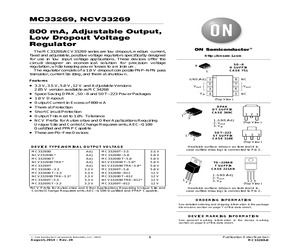
2 7 3 6 4 5 NC Vout NC (Top View) DPAK DT SUFFIX CASE 369C 1 3 1. GND/Adj 2. Vout 3. Vin 1 3 SOT-223 ST SUFFIX CASE 318E 1 2 3 (Top View) 1 2 3 (Top View) DEVICE TYPE/NOMINAL OUTPUT VOLTAGE MC33269D NCV33269D* MC33269DT NCV33269DTRK* MC33269T MC33269D-3.3 MC33269DT-3.3 NCV33269DTRK-3.3* MC33269T-3.3 MC33269ST-3.3 Adj Adj Adj Adj Adj 3.3 V 3.3 V 3.3 V 3.3 V 3.3 V MC33269T-3.5 MC33269D-5.0 MC33269DT-5.0 NCV33269DT-5.0* NCV33269DTRK-5.0* MC33269T-5.0 MC33269D-012 MC33269DT-012 NCV33269DTRK-012* MC33269T-012 3.5 V 5.0 V 5.0 V 5.0 V 5.0 V 5.0 V 12 V 12 V 12 V 12 V *NCV Prefix for Automotive and Other Applications Requiring Unique Site and Control Change Requirements; AEC-Q100 Qualified and PPAP Capable. Heatsink surface (shown as terminal 4 in case outline drawing) is connected to Pin 2. TO-220AB T SUFFIX CASE 221AB 1 2 3 1. GND/Adj 2. Vout 3. Vin 12 3 (Top View) Heatsink surface (shown as terminal 4 in case outline drawing) is connected to Pin 2. ORDERING INFORMATION See detailed ordering and shippin
 13 Pages, 163 KB, Original
0.0022uF C49 0.0022uF ANA0 C Freescale Semiconductor, Inc... 1 2 3 4 Freescale Semiconductor, Inc. MOTOROLA 1 2 3 +3.3V TP6 +3.3V TEST POINT +3.3V TP11 +3.3V TEST POINT 1 3 A +3.3VA TP5 +3.3VA TEST POINT +12V TP9 +12.0V TEST POINT +3.3V +5.0V VOUT VOUT L6 MC33269DT-3.3 GND VIN U13 DNP FM4001 D3 2 - 1 + 4 2 + 1 C47 47uF 10VDC D1 TP1 GROUND TEST POINT TP10 GROUND TEST POINT FERRITE BEAD 2 P3 3 4 1 4 1 1 1 1 3 B B TP2 GROUND TEST POINT C12 0.1uF 0 Ohm R75 FERRITE BEAD L3 + C43 470uF 16VDC +12V EXTERNAL POWER INPUT 7-12V DC/AC 1 + VCC U12 FM4001 D2 4 2 +3.3VA +5.0V 1 3 C 2 3 1 VOUT VOUT NR VOUT TP4 C +5.0V TP7 B Size Title L5 0 Ohm C48 10uF 6VDC R69 + D VDDcore 2 3 MC33269 1 4 3.3V AND 5.0V REGULATOR Designer: DSPO Design E 13 1.1 Rev. FAX: (480) 413-2510 Sheet 12 of (480) 413-5090 2100 East Elliot Road Tempe, Arizona 85284 DSP Standard Products Division REG113NA3/3K 4 5 3.0V REF REGULATOR 1 2 3 1 2 J14 E NOTE: To use, provide +2.5VDC on pin-1. Add 0 OHM resistors for VCAP1, VCAP2, VCAP3 and VCAP4, a
 68 Pages, 737 KB, Original
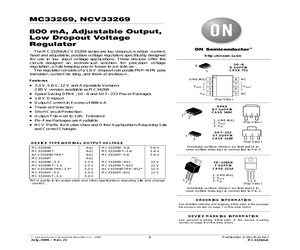
*NCV prefix is for automotive and other applications requiring site and change control. NC (Top View) DEVICE TYPE/NOMINAL OUTPUT VOLTAGE Adj Adj Adj Adj 3.3 V 3.3 V 3.3 V 3.3 V 3.3 V Vout (Top View) 1 MC33269D MC33269DT NCV33269DTRK* MC33269T MC33269D-3.3 MC33269DT-3.3 NCV33269DTRK-3.3* MC33269T-3.3 MC33269ST-3.3 NC TO-220AB T SUFFIX CASE 221AB 1 2 3 1. GND/Adj 2. Vout 3. Vin 12 3 (Top View) Heatsink surface (shown as terminal 4 in case outline drawing) is connected to Pin 2. ORDERING INFORMATION See detailed ordering and shipping information in the package dimensions section on page 7 of this data sheet. DEVICE MARKING INFORMATION See general marking information in the device marking section on page 9 of this data sheet. (c) Semiconductor Components Industries, LLC, 2010 August, 2010 - Rev. 25 1 Publication Order Number: MC33269/D MC33269, NCV33269 MAXIMUM RATINGS Rating Symbol Value Unit Vin 20 V PD qJA qJC PD qJA qJC PD qJA qJC PD qJA qJC Internally Limited 92 6.0 Internally Limited 160 25 Int
 13 Pages, 201 KB, Original
369C 1 3 1. GND/Adj 2. Vout 3. Vin 3 SOT-223 ST SUFFIX CASE 318E NC 1 2 3 (Top View) 1 2 3 (Top View) DEVICE TYPE/NOMINAL OUTPUT VOLTAGE Adj Adj Adj Adj 3.3 V 3.3 V 3.3 V 3.3 V 3.3 V Vout (Top View) 1 MC33269D MC33269DT NCV33269DTRK* MC33269T MC33269D-3.3 MC33269DT-3.3 NCV33269DTRK-3.3* MC33269T-3.3 MC33269ST-3.3 NC MC33269D-5.0 MC33269DT-5.0 MC33269T-5.0 5.0 V 5.0 V 5.0 V Heatsink surface (shown as terminal 4 in case outline drawing) is connected to Pin 2. MC33269D-012 MC33269DT-012 NCV33269DTRK-012* MC33269T-012 12 V 12 V 12 V 12 V TO-220AB T SUFFIX CASE 221AB *NCV prefix is for automotive and other applications requiring site and change control. 1 2 3 1. GND/Adj 2. Vout 3. Vin 12 3 (Top View) Heatsink surface (shown as terminal 4 in case outline drawing) is connected to Pin 2. ORDERING INFORMATION See detailed ordering and shipping information in the package dimensions section on page 7 of this data sheet. DEVICE MARKING INFORMATION See general marking information in the device marking section
 13 Pages, 169 KB, Original
369C 1 3 1. GND/Adj 2. Vout 3. Vin 3 SOT-223 ST SUFFIX CASE 318E NC 1 2 3 (Top View) 1 2 3 (Top View) DEVICE TYPE/NOMINAL OUTPUT VOLTAGE Adj Adj Adj Adj 3.3 V 3.3 V 3.3 V 3.3 V 3.3 V Vout (Top View) 1 MC33269D MC33269DT NCV33269DTRK* MC33269T MC33269D-3.3 MC33269DT-3.3 NCV33269DTRK-3.3* MC33269T-3.3 MC33269ST-3.3 NC MC33269D-5.0 MC33269DT-5.0 MC33269T-5.0 5.0 V 5.0 V 5.0 V Heatsink surface (shown as terminal 4 in case outline drawing) is connected to Pin 2. MC33269D-012 MC33269DT-012 NCV33269DTRK-012* MC33269T-012 12 V 12 V 12 V 12 V TO-220AB T SUFFIX CASE 221A *NCV prefix is for automotive and other applications requiring site and change control. 1 2 3 1. GND/Adj 2. Vout 3. Vin 12 3 (Top View) Heatsink surface (shown as terminal 4 in case outline drawing) is connected to Pin 2. ORDERING INFORMATION See detailed ordering and shipping information in the package dimensions section on page 7 of this data sheet. DEVICE MARKING INFORMATION See general marking information in the device marking section
 13 Pages, 155 KB, Original
369C 1 3 1. GND/Adj 2. Vout 3. Vin 3 SOT-223 ST SUFFIX CASE 318E NC 1 2 3 (Top View) 1 2 3 (Top View) DEVICE TYPE/NOMINAL OUTPUT VOLTAGE Adj Adj Adj Adj 3.3 V 3.3 V 3.3 V 3.3 V 3.3 V Vout (Top View) 1 MC33269D MC33269DT NCV33269DTRK* MC33269T MC33269D-3.3 MC33269DT-3.3 NCV33269DTRK-3.3* MC33269T-3.3 MC33269ST-3.3 NC MC33269D-5.0 MC33269DT-5.0 5.0 V 5.0 V MC33269T-5.0 MC33269D-12 MC33269DT-12 NCV33269DTRK-12* MC33269T-12 5.0 V 12 V 12 V 12 V 12 V *NCV prefix is for automotive and other applications requiring site and change control. Heatsink surface (shown as terminal 4 in case outline drawing) is connected to Pin 2. TO-220AB T SUFFIX CASE 221A 1 2 3 1. GND/Adj 2. Vout 3. Vin 12 3 (Top View) Heatsink surface (shown as terminal 4 in case outline drawing) is connected to Pin 2. ORDERING INFORMATION See detailed ordering and shipping information in the package dimensions section on page 8 of this data sheet. DEVICE MARKING INFORMATION See general marking information in the device marking section on p
 14 Pages, 166 KB, Original
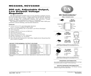
*NCV prefix is for automotive and other applications requiring site and change control. NC (Top View) DEVICE TYPE/NOMINAL OUTPUT VOLTAGE Adj Adj Adj Adj 3.3 V 3.3 V 3.3 V 3.3 V 3.3 V Vout (Top View) 1 MC33269D MC33269DT NCV33269DTRK* MC33269T MC33269D-3.3 MC33269DT-3.3 NCV33269DTRK-3.3* MC33269T-3.3 MC33269ST-3.3 NC TO-220AB T SUFFIX CASE 221AB 1 2 3 1. GND/Adj 2. Vout 3. Vin 12 3 (Top View) Heatsink surface (shown as terminal 4 in case outline drawing) is connected to Pin 2. ORDERING INFORMATION See detailed ordering and shipping information in the package dimensions section on page 7 of this data sheet. DEVICE MARKING INFORMATION See general marking information in the device marking section on page 9 of this data sheet. (c) Semiconductor Components Industries, LLC, 2008 May, 2008 - Rev. 24 1 Publication Order Number: MC33269/D MC33269, NCV33269 MAXIMUM RATINGS Rating Symbol Value Unit Vin 20 V PD qJA qJC PD qJA qJC PD qJA qJC PD qJA qJC Internally Limited 92 6.0 Internally Limited 160 25 Intern
 13 Pages, 202 KB, Original
E BEAD L4 + C1 470uF 16VDC +12V L5 C5 47uF 10VDC TP1 GROUND TEST POINT + B TP2 GROUND TEST POINT C21 0.1uF + VCC U12 VOUT VOUT MC33269DT-5.0 GND VIN +3.3V Typ 135mA 1 3 FM4001 D2 4 2 +5.0V +5.0V 2 3 1 1 3 C VOUT VOUT NR VOUT REG113NA-3.3/3K GND EN VIN U15 MC33269DT-3.3 GND VIN U13 DNP FM4001 D3 FERRITE BEAD L1 TP6 C +5.0V TP7 B Size Title L2 C75 10uF 6VDC + C4 47uF 10VDC 1 2 JG18 +3.3VA +VREFH Single trace to GNDA. R66 0 Ohm +2.5V Input +2.5V Ground Reference MC56F8367EVM.DSN D 4 5 2 3 MC33269 1 4 3.3V AND 5.0V REGULATOR Designer: DSCO Design (512) 895-7215 E Sheet 13 of 14 FAX: (480) 413-2510 2100 East Elliot Road Tempe, Arizona 85284 1.0 Rev. Digital Signal Controller Operation REG113NA3/3K 1 2 3 3.3V REF REGULATOR POWER GOOD LED E LED13 GREEN LED R64 270 +5.0V NOTE: Remove 0 OHM resistor to use Analog GND isolation jumper. External +2.5V Power Supply Input 1 2 J24 Date: Thursday, September 02, 2004 Document Number D +2.5V POWER SUPPLIES + 10 Ohm R65 FERRITE BEAD L3 FERRITE BEAD C2 47uF 10VDC +
 80 Pages, 485 KB, Original
E BEAD L4 + C1 470uF 16VDC +12V L5 C5 47uF 10VDC TP1 GROUND TEST POINT + B TP2 GROUND TEST POINT C21 0.1uF + VCC U12 VOUT VOUT MC33269DT-5.0 GND VIN +3.3V Typ 135mA 1 3 FM4001 D2 4 2 +5.0V +5.0V 2 3 1 1 3 C VOUT VOUT NR VOUT REG113NA-3.3/3K GND EN VIN U15 MC33269DT-3.3 GND VIN U13 DNP FM4001 D3 FERRITE BEAD L1 TP6 C +5.0V TP7 B Size Title L2 C75 10uF 6VDC + C4 47uF 10VDC 1 2 JG18 +3.3VA +VREFH Single trace to GNDA. R66 0 Ohm +2.5V Input +2.5V Ground Reference MC56F8367EVM.DSN D 4 5 2 3 MC33269 1 4 3.3V AND 5.0V REGULATOR Designer: DSCO Design (512) 895-7215 E Sheet 13 of 14 FAX: (480) 413-2510 2100 East Elliot Road Tempe, Arizona 85284 1.0 Rev. Digital Signal Controller Operation REG113NA3/3K 1 2 3 3.3V REF REGULATOR POWER GOOD LED E LED13 GREEN LED R64 270 +5.0V NOTE: Remove 0 OHM resistor to use Analog GND isolation jumper. External +2.5V Power Supply Input 1 2 J24 Date: Thursday, September 02, 2004 Document Number D +2.5V POWER SUPPLIES + 10 Ohm R65 FERRITE BEAD L3 FERRITE BEAD C2 47uF 10VDC +
 80 Pages, 791 KB, Original
1.0% Tolerance http://onsemi.com SOP-8 D SUFFIX CASE 751 8 1 Gnd/Adj Vout Vin 1 8 2 7 3 6 4 5 NC DPAK DT SUFFIX CASE 369A 1 Adj Adj Adj 3.3 V 3.3 V 3.3 V 3.3 V Vout (Top View) 3 DEVICE TYPE / NOMINAL OUTPUT VOLTAGE MC33269D MC33269DT MC33269T MC33269D-3.3 MC33269DT-3.3 MC33269T-3.3 MC33269ST-3.3 NC MC33269D-5.0 MC33269DT-5.0 MC33269T-5.0 MC33269D-12 MC33269DT-12 MC33269T-12 5.0 V 5.0 V 5.0 V 12 V 12 V 12 V 1. Gnd/Adj 2. Vout 1 2 3 3. Vin SOT-223 ST SUFFIX CASE 318E (Top View) 1 3 Heatsink surface (shown as terminal 4 in case outline drawing) is connected to Pin 2. TO-220AB T SUFFIX CASE 221A 1 Pin: 1. 2. 3. 2 3 Gnd/Adj Vout Vin 1 2 3 (Top View) Heatsink surface (shown as terminal 4 in case outline drawing) is connected to Pin 2. ORDERING INFORMATION See detailed ordering and shipping information in the package dimensions section on page 7 of this data sheet. Semiconductor Components Industries, LLC, 2000 April, 2000 - Rev. 8 1 Publication Order Number: MC33269/D MC33269 MAXIMUM RATINGS Rating Pow
 16 Pages, 145 KB, Original
E BEAD L4 + C1 470uF 16VDC +12V L5 C5 47uF 10VDC TP1 GROUND TEST POINT + B TP2 GROUND TEST POINT C21 0.1uF + VCC U12 VOUT VOUT MC33269DT-5.0 GND VIN +3.3V Typ 135mA 1 3 FM4001 D2 4 2 +5.0V +5.0V 2 3 1 1 3 C VOUT VOUT NR VOUT REG113NA-3.3/3K GND EN VIN U15 MC33269DT-3.3 GND VIN U13 DNP FM4001 D3 FERRITE BEAD L1 TP6 C +5.0V TP7 B Size Title L2 C75 10uF 6VDC + C4 47uF 10VDC 1 2 JG18 +3.3VA +VREFH Single trace to GNDA. R66 0 Ohm +2.5V Input +2.5V Ground Reference MC56F8357EVM.DSN D 4 5 2 3 MC33269 1 4 3.3V AND 5.0V REGULATOR Designer: DSPD Design E 14 1.0 Rev. FAX: (480) 413-2510 Sheet 13 of (480) 413-5090 2100 East Elliot Road Tempe, Arizona 85284 DSP Standard Products Division REG113NA3/3K 1 2 3 3.3V REF REGULATOR POWER GOOD LED E LED13 GREEN LED R64 270 +5.0V NOTE: Remove 0 OHM resistor to use Analog GND isolation jumper. External +2.5V Power Supply Input 1 2 J24 Date: Wednesday, June 04, 2003 Document Number D +2.5V POWER SUPPLIES + 10 Ohm R65 FERRITE BEAD L3 FERRITE BEAD C2 47uF 10VDC +3.3V + +5
 76 Pages, 722 KB, Original
369A 1 3 1. GND/Adj 2. Vout 3. Vin 3 SOT-223 ST SUFFIX CASE 318E NC 1 2 3 (Top View) 1 2 3 (Top View) DEVICE TYPE/NOMINAL OUTPUT VOLTAGE Adj Adj Adj Adj 3.3 V 3.3 V 3.3 V 3.3 V 3.3 V Vout (Top View) 1 MC33269D MC33269DT NCV33269DTRK* MC33269T MC33269D-3.3 MC33269DT-3.3 NCV33269DTRK-3.3* MC33269T-3.3 MC33269ST-3.3 NC MC33269D-5.0 MC33269DT-5.0 5.0 V 5.0 V MC33269T-5.0 MC33269D-12 MC33269DT-12 NCV33269DTRK-12* MC33269T-12 5.0 V 12 V 12 V 12 V 12 V *NCV prefix is for automotive and other applications requiring site and change control. Heatsink surface (shown as terminal 4 in case outline drawing) is connected to Pin 2. TO-220AB T SUFFIX CASE 221A 1 2 3 1. GND/Adj 2. Vout 3. Vin 12 3 (Top View) Heatsink surface (shown as terminal 4 in case outline drawing) is connected to Pin 2. ORDERING INFORMATION See detailed ordering and shipping information in the package dimensions section on page 8 of this data sheet. DEVICE MARKING INFORMATION See general marking information in the device marking section on p
 14 Pages, 156 KB, Original
 C55 0.0022uF C53 0.0022uF C51 0.0022uF C49 0.0022uF ANA0 C 1 2 3 4 56F8323EVM Schematics, Rev. 2 1 2 3 4 +3.3V TP6 +3.3V TEST POINT +3.3V TP11 +3.3V TEST POINT 1 1 1 3 A +3.3VA TP5 +3.3VA TEST POINT +12V TP9 +12.0V TEST POINT +3.3V +5.0V U13 VOUT VOUT L6 MC33269DT-3.3 GND VIN D3 2 - 1 DNP FM4001 3 + 4 2 + 1 C47 47uF 10VDC D1 TP1 GROUND TEST POINT TP10 GROUND TEST POINT FERRITE BEAD 2 P3 4 1 1 1 1 3 B TP2 GROUND TEST POINT C12 0.1uF 0 Ohm R75 FERRITE BEAD L3 + C43 470uF 16VDC +12V EXTERNAL POWER INPUT 7-12V DC/AC 1 + VCC U12 FM4001 D2 4 2 +3.3VA +5.0V 1 3 C 2 3 1 VOUT VOUT NR VOUT TP4 C +5.0V TP7 B Size Title L5 0 Ohm C48 10uF 6VDC R69 + D VDDcore 2 3 MC33269 1 4 3.3V AND 5.0V REGULATOR Designer: DSPO Design E 13 1.1 Rev. FAX: (480) 413-2510 Sheet 12 of (480) 413-5090 2100 East Elliot Road Tempe, Arizona 85284 DSP Standard Products Division REG113NA3/3K 4 5 3.0V REF REGULATOR 1 2 3 1 2 J14 E NOTE: To use, provide +2.5VDC on pin-1. Add 0 OHM resistors for VCAP1, VCAP2, VCAP3 and VCAP4, and remove
 72 Pages, 2014 KB, Original
369C 1 3 1. GND/Adj 2. Vout 3. Vin 3 SOT-223 ST SUFFIX CASE 318E NC 1 2 3 (Top View) 1 2 3 (Top View) DEVICE TYPE/NOMINAL OUTPUT VOLTAGE Adj Adj Adj Adj 3.3 V 3.3 V 3.3 V 3.3 V 3.3 V Vout (Top View) 1 MC33269D MC33269DT NCV33269DTRK* MC33269T MC33269D-3.3 MC33269DT-3.3 NCV33269DTRK-3.3* MC33269T-3.3 MC33269ST-3.3 NC MC33269D-5.0 MC33269DT-5.0 5.0 V 5.0 V MC33269T-5.0 MC33269D-12 MC33269DT-12 NCV33269DTRK-12* MC33269T-12 5.0 V 12 V 12 V 12 V 12 V *NCV prefix is for automotive and other applications requiring site and change control. Heatsink surface (shown as terminal 4 in case outline drawing) is connected to Pin 2. TO-220AB T SUFFIX CASE 221A 1 2 3 1. GND/Adj 2. Vout 3. Vin 12 3 (Top View) Heatsink surface (shown as terminal 4 in case outline drawing) is connected to Pin 2. ORDERING INFORMATION See detailed ordering and shipping information in the package dimensions section on page 8 of this data sheet. DEVICE MARKING INFORMATION See general marking information in the device marking section on p
 14 Pages, 156 KB, Original
dj Adj Adj Adj 3.3 V 3.3 V 3.3 V 3.3 V 3.3 V MC33269D-5.0 MC33269DT-5.0 5.0 V 5.0 V MC33269T-5.0 MC33269D-12 MC33269DT-12 NCV33269DTRK-12* MC33269T-12 5.0 V 12 V 12 V 12 V 12 V NC Vout NC (Top View) 3 MC33269D MC33269DT NCV33269DTRK* MC33269T MC33269D-3.3 MC33269DT-3.3 NCV33269DTRK-3.3* MC33269T-3.3 MC33269ST-3.3 SO-8 D SUFFIX CASE 751 8 1 3 SOT-223 ST SUFFIX CASE 318E 1 2 3 (Top View) 1 2 3 (Top View) Heatsink surface (shown as terminal 4 in case outline drawing) is connected to Pin 2. TO-220AB T SUFFIX CASE 221A *NCV prefix is for automotive and other applications requiring site and change control. 1 2 3 1. GND/Adj 2. Vout 3. Vin 12 3 (Top View) Heatsink surface (shown as terminal 4 in case outline drawing) is connected to Pin 2. ORDERING INFORMATION See detailed ordering and shipping information in the package dimensions section on page 8 of this data sheet. DEVICE MARKING INFORMATION See general marking information in the device marking section on page 9 of this data sheet. Semiconductor Comp
 14 Pages, 135 KB, Original


