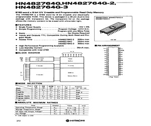
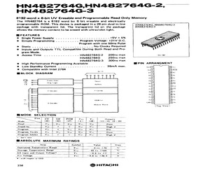
HN482764G-3 8192-word x 8-bit UV Erasable and Programmable Read Only Memory The HN482764 is a 8192 word by 8 bit erasable and electrically programmable ROM. This device is packaged in a 28 pin dual-in-line package with transparent lid. The transparent lid on the package allows the memory content to be erased with ultraviolet light. W@FEATURES @ Single Power Supply .......0... 0000 eee wees +5V + 5% @ Simple Programming .......... Program Voltage: +21V D.C. Program with one 50ms Pulse @ Static... ee eee No Clocks Required @ Inputs and Outputs TTL Compatible During Both Read and Pro- gram Mode. @ Access Time ........-..-.6- HN482764G-2 200ns max HN482764G 250ns max HN482764G-3 300ns max @ High Performance Programming Available @ Low Standby Current ..............02.00. 35mA max. Compatible with Intel 2764 Oy ~ Or BMBLOCK DIAGRAM oN FGM Power Down oF Peng. Logic Our cE Buffers Y-Gating . 65536 bit Au Memory Matrix MIMODE SELECTION Pins CE OE PGM Vep Vec Outputs Mode (20) (22) (27) (1) (
 5 Pages, 252 KB, Scan
HN482764G-3 8192-word x 8-bit UV Erasable and Programmable Read Only Memory The HN482764 is a 8192 word by 8 bit erasable and electrically programmable ROM. This device is packaged in a 28 pin dual-in-line package with transparent lid. The transparent lid on the package allows the memory content to be erased with ultraviolet light. M FEATURES Single Power Supply Simple Programming Static gram Mode. Access Time High Performance Programming Available Low Standby Current De eee eee ete +5V + 5% Program Voltage: +21V D.C. Program with one 50ms Pulse Inputs and Outputs TTL Compatible During Both Read and Pro- HN482764G-2 HN482764G }IN482764G, HN482764G-2 HIN482764G-3 No Clocks Required 200ns max i 250ns max (DG-28) HN482764G-3 300ns max Compatible with Intel 2764 MBLOCK DIAGRAM 1 1g lz c cA Power Down Prog. Logic Y-Decoder MIMODE SELECTION BIPIN ARRANGMENT 35mA max. ver cl ks Veo an? | [27] PGM an * a(S] [26] NC as (a (25] as as[5] [24] As Output a [6] [23] An Buffers af] 123] 3E a: [8] [
 5 Pages, 140 KB, Scan
O Clock synchronous HD61100A SCI 10-digit X 8-segment LCD 12 External Expansion HD6301YO (HD6303Y) External expansion function HD6301YO HD6321, HN27C64 HD63S0, HM6264 H2S71 200 13 Slow Device Interface HD63B01YO MR pin External expansion function HD6301YO HN482764G-3 HM6264LP 233 14 Low Power Dissipation Mode HD6301YO Low power dissipation mode (standbY) \sleep HD6301YO 247 188 I/O port (Portl) port3 port6 lS HA183SP Control and Error Detection HD6301YO Trap function HD6301YO I/O port (PortS)HA183SP port7 ~HITACHI 848 264 SECTION 1. 1.1 HD61830 (IM200) GRAPHIC MODE HARDWARE DESCRIPTION 1.1.1 Function Initializes graphic mode and displays dot graphics on the LM200 liquid crystal module. 1.1.2 Microcomputer Operation The HD6301YO transfers display data to the dot matrix liquid crystal graphic display controller LSI HD61830 (LCTC) from port 3 onto the LCTC data bus (DBO ~ through port 1. 1.1.3 DE7), and transmits control signals E, R/W, and RS Ports 1 and 3 are controlled by software. Peripheral Dev
 1338 Pages, 53109 KB, Original
6-word x 8-bit U.V. Erasable & HN482732AG-30 4096-word x 8-bit U.V. Erasable & HN482764 8192-word x 8-bit U.V. Erasable & HN482764-3 8192-word x 8-bit U.V. Erasable & HN482764-4 8192-word x 8-bit U.V. Erasable & HN482764G 8192-word x 8-bit U.V. Erasable & HN482764G-3 8192-word x 8-bit U.V. Erasable & HN482764G-4 8192-word x 8-bit U.V. Erasable & Electrically Electrically Electrically Electrically Electrically Electrically Electrically Electrically Electrically Electrically Electrically Electrically Electrically HN4827128G-25 PROM (NMOS) 318 PROM (NMOS) 318 PROM (NMOS) 322 PROM (NMOS) 325 PROM (NMOS) 325 PROM (NMOS) 325 PROM (NMOS) 328 PROM (NMOS) - PROM (NMOS) 328 PROM (NMOS) 328 PROM (NMOS) 328 PROM (NMOS) 328 PROM (NMOS) 332 PROM (NMOS) 332 HN4827128G-45 16384-word x 8-bit U.V. Erasable & HN48016P 2048-word x 8-bit Electrically Electrically PROM (NMOS) PROM (NMOS) Bipolar RAM HM10414 328 16384-word x 8-bit U.V. Erasable & Electrically * 314 16384-word x 8-bit U.V. Erasable & Electrically HN4827
 447 Pages, 126941 KB, Original
6264LFP-12 HM6264LFP-15 HM6267P-35 HM6267P-45 HM6810P HM68AI0P B A A A A A A A A A A A A A A A A A B B B B A A A A HN27256-20 HN27256-25 HN27256-30 HN27C64-15 HN27C64-20 HN27C64-25 HN27C64-30 HN482732AG-20 HN482732AG-25 HN482732AG-30 HN482764G HN482764G-2 HN482764G-3 HN482764G-4 HN482764P-3 HN4827128G-25 HN4827128G-30 HN4827128G-45 HN4827128P-30 HN58064P-25 HN58064P-30 HN58064P-45 HN61256P HN61256FP HN61364P HN61364FP Access Time (ns)max Function 55 45 55 45 55 45 55 70 45 55 70 45 55 70 100 120 150 120 150 100 120 150 120 150 35 45 450 360 16384 x 1 Static RAM 4096 x 4 Static RAM 8192 x 8 Static RAM 16384 x 1 Static RAM 128 x 8 Static RAM 200 250 300 150 200 250 300 200 250 300 250 200 300 450 300 250 300 450 300 250 300 450 32768 x 8 EPROM 8192 x 8 EPROM 4096 x 8 EPROM 8192 x 8 EPROM 8192 x 8 One Time PROM 16384 x 8 EPROM 16384 x 8 One Time PROM 8192 x 8 EEPROM 32768 x 8 or 65536 x 4 Mask ROM 3500 8192 x 8 Mask ROM 250 Structure Material for details Page DB 36 DP-20 CG-20 DP-20 DG-20 DP-20 CMOS
 51 Pages, 18673 KB, Original


