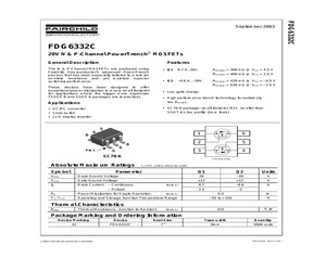
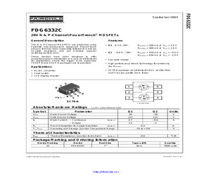
FDG6332C 20V N & P-Channel PowerTrench MOSFETs General Description Features The N & P-Channel MOSFETs are produced using Fairchild Semiconductor's advanced PowerTrench process that has been especially tailored to minimize on-state resistance and yet maintain superior switching performance. * Q1 0.7 A, 20V. RDS(ON) = 300 m @ VGS = 4.5 V RDS(ON) = 400 m @ VGS = 2.5 V * Q2 -0.6 A, -20V. RDS(ON) = 420 m @ VGS = -4.5 V RDS(ON) = 630 m @ VGS = -2.5 V These devices have been designed to offer exceptional power dissipation in a very small footprint for applications where the bigger more expensive TSSOP-8 and SSOP-6 packages are impractical. * Low gate charge * High performance trench technology for extremely low RDS(ON) Applications * SC70-60 package: small footprint (51% smaller than * DC/DC converter * Load switch * LCD display inverter SSOT-6); low profile (1mm thick) S G D D 1 6 2 5 3 4 G Pin 1 S SC70-6 Complementary Absolute Maximum Ratings Symbol o TA=25 C unless otherwise noted Q1 Q2 Units VDSS Dr
 11 Pages, 221 KB, Original
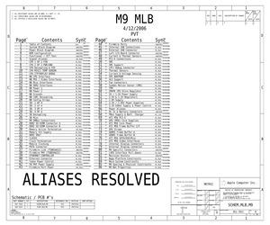
T III NOT TO REVEAL OR PUBLISH IN WHOLE OR PART SIZE APPLE COMPUTER INC. DRAWING NUMBER SCALE SHT NONE 8 7 6 5 4 3 2 REV. 051-7023 D 40 1 OF B 86 A 8 6 7 2 3 4 5 1 D D Yukon Power Control Allows powering Yukon down during battery sleep to save power Q4300 FDG6332C_NL SC70-6 P-CHN PP3V3_S3 62 59 58 56 51 45 37 32 27 5 80 66 64 63 PP3V3_S3AC D S 4 5 39 66 3 G 5 PPVIN_S3_P2V5S3_SVIN 1 R4305 100K 100K 5% 1/16W MF-LF 2 402 5% 1/16W MF-LF 2 402 PM_SLP_S3BATT_L P2V5S3_EN_L 62 41 P2V5S3_EN_L MAKE_BASE=TRUE 3 Q4304 D 2N7002DW-X-F 5 G 2 4 68 66 64 63 61 60 54 47 43 5 78 70 C 2N7002DW-X-F SOT-363 S 41 62 6 Q4304 D C 62 1 R4304 G SOT-363 S 1 PPBUS_G3H P1V2S3_RUNSS 5 62 1.2V enable has pull-up to 3.3V 1 R4302 470K 3 5% 1/16W MF-LF 2 402 2N7002 PM_SLP_S3BATT 5 Q4302 D 1 G SOT23-LF S 2 6 D PM_SLP_S4_L ENETPWR_S3AC N-CHN 65 63 50 47 46 23 5 2 G FWPWR_EN_L 1 0 2 FDG6332C_NL SC70-6 1 R4300 43 Q4300 S FWPWR_EN_L_OR_GND ENETPWR_S3 5% 1/16W MF-LF 402 1 R4301 0 5% 1/16W MF-LF 2 402 B B When ENETPWR_S3AC B
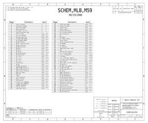
 86 Pages, 1693 KB, Original
FDG6332C 20V N & P-Channel PowerTrench MOSFETs General Description Features The N & P-Channel MOSFETs are produced using Fairchild Semiconductor's advanced PowerTrench process that has been especially tailored to minimize on-state resistance and yet maintain superior switching performance. * Q1 0.7 A, 20V. RDS(ON) = 300 m @ VGS = 4.5 V RDS(ON) = 400 m @ VGS = 2.5 V * Q2 -0.6 A, -20V. RDS(ON) = 420 m @ VGS = -4.5 V RDS(ON) = 630 m @ VGS = -2.5 V These devices have been designed to offer exceptional power dissipation in a very small footprint for applications where the bigger more expensive TSSOP-8 and SSOP-6 packages are impractical. * Low gate charge * High performance trench technology for extremely low RDS(ON) Applications * SC70-6 package: small footprint (51% smaller than * DC/DC converter * Load switch * LCD display inverter SSOT-6); low profile (1mm thick) S G D D 1 6 2 5 3 4 G Pin 1 S SC70-6 Complementary Absolute Maximum Ratings Symbol o TA=25 C unless otherwise noted Q1 Q2 VDSS Drain-Sou
 8 Pages, 92 KB, Original
FDG6332C 20V N & P-Channel PowerTrench MOSFETs General Description Features The N & P-Channel MOSFETs are produced using Fairchild Semiconductor's advanced PowerTrench process that has been especially tailored to minimize on-state resistance and yet maintain superior switching performance. * Q1 0.7 A, 20V. RDS(ON) = 300 m @ VGS = 4.5 V RDS(ON) = 400 m @ VGS = 2.5 V * Q2 -0.6 A, -20V. RDS(ON) = 420 m @ VGS = -4.5 V RDS(ON) = 630 m @ VGS = -2.5 V These devices have been designed to offer exceptional power dissipation in a very small footprint for applications where the bigger more expensive TSSOP-8 and SSOP-6 packages are impractical. * Low gate charge * High performance trench technology for extremely low RDS(ON) Applications * SC70-6 package: small footprint (51% smaller than * DC/DC converter * Load switch * LCD display inverter SSOT-6); low profile (1mm thick) S G D D 1 6 2 5 3 4 G Pin 1 S SC70-6 Complementary Absolute Maximum Ratings Symbol o TA=25 C unless otherwise noted Q1 Q2 VDSS Drain-Sou
 8 Pages, 96 KB, Original
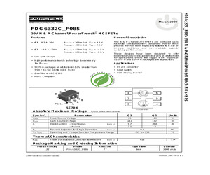
ges that ON Semiconductor was negligent regarding the design or manufacture of the part. ON Semiconductor is an Equal Opportunity/Affirmative Action Employer. This literature is subject to all applicable copyright laws and is not for resale in any manner. FDG6332C_F085 20V N & P-Channel PowerTrench MOSFETs General Description Features * Q1 0.7 A, 20V. The N & P-Channel MOSFETs are produced using Fairchild Semiconductor's advanced PowerTrench process that has been especially tailored to minimize on-state resistance and yet maintain superior switching performance. RDS(ON) = 300 m @ VGS = 4.5 V RDS(ON) = 400 m @ VGS = 2.5 V * Q2 -0.6 A, -20V. RDS(ON) = 420 m @ VGS = -4.5 V RDS(ON) = 630 m @ VGS = -2.5 V These devices have been designed to offer exceptional power dissipation in a very small footprint for applications where the bigger more expensive TSSOP-8 and SSOP-6 packages are impractical. * Low gate charge * High performance trench technology for extremely Applications low RDS(ON) * DC/DC convert
 10 Pages, 371 KB, Original
FDG6332C 20V N & P-Channel PowerTrench MOSFETs General Description Features The N & P-Channel MOSFETs are produced using Fairchild Semiconductor's advanced PowerTrench process that has been especially tailored to minimize on-state resistance and yet maintain superior switching performance. * Q1 0.7 A, 20V. RDS(ON) = 300 m @ VGS = 4.5 V RDS(ON) = 400 m @ VGS = 2.5 V * Q2 -0.6 A, -20V. RDS(ON) = 420 m @ VGS = -4.5 V RDS(ON) = 630 m @ VGS = -2.5 V These devices have been designed to offer exceptional power dissipation in a very small footprint for applications where the bigger more expensive TSSOP-8 and SSOP-6 packages are impractical. * Low gate charge * High performance trench technology for extremely low RDS(ON) Applications * SC70-6 package: small footprint (51% smaller than * DC/DC converter * Load switch * LCD display inverter SSOT-6); low profile (1mm thick) S G D D 1 6 2 5 3 4 G Pin 1 S SC70-6 Complementary Absolute Maximum Ratings Symbol o TA=25 C unless otherwise noted Q1 Q2 Units VDSS Dra
 8 Pages, 89 KB, Original
FDG6332C_F085 20V N & P-Channel PowerTrench MOSFETs General Description Features * Q1 0.7 A, 20V. The N & P-Channel MOSFETs are produced using Fairchild Semiconductor's advanced PowerTrench process that has been especially tailored to minimize on-state resistance and yet maintain superior switching performance. RDS(ON) = 300 m @ VGS = 4.5 V RDS(ON) = 400 m @ VGS = 2.5 V * Q2 -0.6 A, -20V. RDS(ON) = 420 m @ VGS = -4.5 V RDS(ON) = 630 m @ VGS = -2.5 V These devices have been designed to offer exceptional power dissipation in a very small footprint for applications where the bigger more expensive TSSOP-8 and SSOP-6 packages are impractical. * Low gate charge * High performance trench technology for extremely Applications low RDS(ON) * DC/DC converter * SC70-6 package: small footprint (51% smaller than * Load switch SSOT-6); low profile (1mm thick) * LCD display inverter * Qualified to AEC Q101 * RoHS Compliant S G D D 1 6 2 5 3 4 G Pin 1 S SC70-6 Absolute Maximum Ratings Symbol Complementary o TA=25
 10 Pages, 327 KB, Original
FDG6332C_F085 20V N & P-Channel PowerTrench MOSFETs General Description Features * Q1 0.7 A, 20V. The N & P-Channel MOSFETs are produced using Fairchild Semiconductor's advanced PowerTrench process that has been especially tailored to minimize on-state resistance and yet maintain superior switching performance. RDS(ON) = 300 m @ VGS = 4.5 V RDS(ON) = 400 m @ VGS = 2.5 V * Q2 -0.6 A, -20V. RDS(ON) = 420 m @ VGS = -4.5 V RDS(ON) = 630 m @ VGS = -2.5 V These devices have been designed to offer exceptional power dissipation in a very small footprint for applications where the bigger more expensive TSSOP-8 and SSOP-6 packages are impractical. * Low gate charge * High performance trench technology for extremely Applications low RDS(ON) * DC/DC converter * SC70-6 package: small footprint (51% smaller than * Load switch SSOT-6); low profile (1mm thick) * LCD display inverter * Qualified to AEC Q101 * RoHS Compliant S G D D 1 6 2 5 3 4 G Pin 1 S SC70-6 Absolute Maximum Ratings Symbol Complementary o TA=25
 8 Pages, 280 KB, Original
I NOT TO REVEAL OR PUBLISH IN WHOLE OR PART SIZE APPLE COMPUTER INC. DRAWING NUMBER D SCALE SHT NONE 8 7 6 5 4 3 2 REV. 051-7150 A.0.0 OF 40 1 84 A 8 6 7 2 3 4 5 1 D D Yukon Power Control Allows powering Yukon down during battery sleep to save power Q4300 FDG6332C_NL SC70-6 65C3 P-CHN =PP3V3_S3_P3V3S3AC 4 =PP3V3_S3AC_FET D S 65D3 3 G 5 PPVIN_S3_P2V5S3_SVIN 1 61D6 R4304 100K 2 5% 1/16W MF-LF 402 =P2V5S3_EN 61D8 PM_SLP_S3BATT_L MAKE_BASE=TRUE 3 D C Q4304 C 2N7002 1 G SOT23-LF S 2 65C1 =PPBUS_G3H_S3AC 1 P1V2S3_RUNSS R4302 2 5D7 61B7 1.2V enable has pull-up to 3.3V 470K 3 5% 1/16W MF-LF 402 D Q4302 2N7002 PM_SLP_S3BATT 1 G SOT23-LF S 2 6 D PM_SLP_S4_L 2 G 1 0 2 FDG6332C_NL SC70-6 1 R4300 FWPWR_EN_L Q4300 S ENETPWR_S3AC 43C7 N-CHN 64B8 49C5 23C3 FWPWR_EN_L_OR_GND ENETPWR_S3 5% 1/16W MF-LF 402 1 R4301 0 B 2 5% 1/16W MF-LF 402 B When ENETPWR_S3AC BOMOPTION is active: State PM_SLP_S4_L PM_SLP_S3BATT PM_SLP_S3BATT_L S0 AC 0V 3.3V 0V (3.3V ON) 3.3V 3.3V (2.5V ON) 3.3V (1.2V ON) S0 Batt 0V 3.3V
 84 Pages, 1477 KB, Original
FDG6332C 20V N & P-Channel PowerTrench MOSFETs General Description Features The N & P-Channel MOSFETs are produced using Fairchild Semiconductor's advanced PowerTrench process that has been especially tailored to minimize on-state resistance and yet maintain superior switching performance. * Q1 0.7 A, 20V. RDS(ON) = 300 m @ VGS = 4.5 V RDS(ON) = 400 m @ VGS = 2.5 V * Q2 -0.6 A, -20V. RDS(ON) = 420 m @ VGS = -4.5 V RDS(ON) = 630 m @ VGS = -2.5 V These devices have been designed to offer exceptional power dissipation in a very small footprint for applications where the bigger more expensive TSSOP-8 and SSOP-6 packages are impractical. * Low gate charge * High performance trench technology for extremely low RDS(ON) Applications * SC70-6 package: small footprint (51% smaller than * DC/DC converter * Load switch * LCD display inverter SSOT-6); low profile (1mm thick) S G D D 1 6 2 5 3 4 G Pin 1 S SC70-6 Complementary Absolute Maximum Ratings Symbol o TA=25 C unless otherwise noted Q1 Q2 VDSS Drain-Sou
 9 Pages, 163 KB, Original
ges that ON Semiconductor was negligent regarding the design or manufacture of the part. ON Semiconductor is an Equal Opportunity/Affirmative Action Employer. This literature is subject to all applicable copyright laws and is not for resale in any manner. FDG6332C 20V N & P-Channel PowerTrench MOSFETs General Description Features The N & P-Channel MOSFETs are produced using Fairchild Semiconductor's advanced PowerTrench process that has been especially tailored to minimize on-state resistance and yet maintain superior switching performance. * Q1 0.7 A, 20V. RDS(ON) = 300 m @ VGS = 4.5 V RDS(ON) = 400 m @ VGS = 2.5 V * Q2 -0.6 A, -20V. RDS(ON) = 420 m @ VGS = -4.5 V RDS(ON) = 630 m @ VGS = -2.5 V These devices have been designed to offer exceptional power dissipation in a very small footprint for applications where the bigger more expensive TSSOP-8 and SSOP-6 packages are impractical. * Low gate charge * High performance trench technology for extremely low RDS(ON) Applications * SC70-6 package: sm
 10 Pages, 277 KB, Original
FDG6332C 20V N & P-Channel PowerTrench MOSFETs General Description Features The N & P-Channel MOSFETs are produced using Fairchild Semiconductor's advanced PowerTrench process that has been especially tailored to minimize on-state resistance and yet maintain superior switching performance. * Q1 0.7 A, 20V. RDS(ON) = 300 m @ VGS = 4.5 V RDS(ON) = 400 m @ VGS = 2.5 V * Q2 -0.6 A, -20V. RDS(ON) = 420 m @ VGS = -4.5 V RDS(ON) = 630 m @ VGS = -2.5 V These devices have been designed to offer exceptional power dissipation in a very small footprint for applications where the bigger more expensive TSSOP-8 and SSOP-6 packages are impractical. * Low gate charge * High performance trench technology for extremely low RDS(ON) Applications * SC70-6 package: small footprint (51% smaller than * DC/DC converter * Load switch * LCD display inverter SSOT-6); low profile (1mm thick) S G D D 1 6 2 5 3 4 G Pin 1 S SC70-6 Complementary Absolute Maximum Ratings Symbol o TA=25 C unless otherwise noted Q1 Q2 VDSS Drain-Sou
 8 Pages, 90 KB, Original
 III NOT TO REVEAL OR PUBLISH IN WHOLE OR PART SIZE APPLE COMPUTER INC. DRAWING NUMBER SCALE SHT NONE 8 7 6 5 4 3 2 REV. 051-7023 D 40 1 OF 06 86 A 8 6 7 2 3 4 5 1 D D Yukon Power Control Allows powering Yukon down during battery sleep to save power Q4300 FDG6332C_NL SC70-6 P-CHN PP3V3_S3 62 59 58 56 51 45 37 32 27 5 80 66 64 63 PP3V3_S3AC D S 4 5 39 66 3 G 5 PPVIN_S3_P2V5S3_SVIN 1 R4305 100K 100K 5% 1/16W MF-LF 2 402 5% 1/16W MF-LF 2 402 PM_SLP_S3BATT_L P2V5S3_EN_L 62 41 P2V5S3_EN_L MAKE_BASE=TRUE 3 Q4304 D 2N7002DW-X-F 5 G 2 4 66 64 63 61 60 54 47 43 5 4 78 70 68 C 2N7002DW-X-F SOT-363 S 41 62 6 Q4304 D C 62 1 R4304 G SOT-363 S 1 PPBUS_G3H P1V2S3_RUNSS 5 62 1.2V enable has pull-up to 3.3V 1 R4302 470K 3 5% 1/16W MF-LF 2 402 2N7002 PM_SLP_S3BATT 5 Q4302 D 1 G SOT23-LF S 2 6 D PM_SLP_S4_L ENETPWR_S3AC N-CHN 65 63 50 47 46 23 5 2 G FWPWR_EN_L 1 0 2 FDG6332C_NL SC70-6 1 R4300 43 Q4300 S FWPWR_EN_L_OR_GND ENETPWR_S3 5% 1/16W MF-LF 402 1 R4301 0 5% 1/16W MF-LF 2 402 B B When ENETPWR_S3AC
 86 Pages, 1697 KB, Original
 III NOT TO REVEAL OR PUBLISH IN WHOLE OR PART SIZE APPLE COMPUTER INC. DRAWING NUMBER SCALE SHT NONE 8 7 6 5 4 3 2 REV. 051-7099 D 42 1 OF D 104 A 8 6 7 2 3 4 5 1 D D Yukon Power Control Allows powering Yukon down during battery sleep to save power Q4300 FDG6332C_NL SC70-6 P-CHN =PP3V3_S3_P3V3S3AC 63 4 =PP3V3_S3AC_FET D S 63 3 G 5 PPVIN_S3_P2V5S3_SVIN 1 R4305 100K 100K 5% 1/16W MF-LF 2 402 5% 1/16W MF-LF 2 402 PM_SLP_S3BATT_L P2V5S3_EN_L =P2V5S3_EN_L MAKE_BASE=TRUE 3 59 6 Q4304 Q4304 D M C D C 59 1 R4304 2N7002DW-X-F 5 G 2 4 63 C 2N7002DW-X-F SOT-363 S G SOT-363 S 1 =PPBUS_G3H_S3AC P1V2S3_RUNSS 5 59 1.2V enable has pull-up to 3.3V 1 R4302 470K 3 5% 1/16W MF-LF 2 402 Q4302 D 2N7002 PM_SLP_S3BATT 1 G SOT23-LF S 2 6 D PM_SLP_S4_L ENETPWR_S3AC N-CHN 62 47 23 2 G FWPWR_EN_L 1 0 2 FDG6332C_NL SC70-6 1 R4300 41 Q4300 S FWPWR_EN_L_OR_GND ENETPWR_S3 5% 1/16W MF-LF 402 1 R4301 N 0 5% 1/16W MF-LF 2 402 B B When ENETPWR_S3AC BOMOPTION is active: State FWPWR_EN_L S0 AC 0V 3.3V 0V (3.3V ON) 3.3V
 79 Pages, 1486 KB, Original
 III NOT TO REVEAL OR PUBLISH IN WHOLE OR PART SIZE APPLE COMPUTER INC. DRAWING NUMBER SCALE SHT NONE 8 7 6 5 4 3 2 REV. 051-7099 D 42 1 OF D 104 A 8 6 7 2 3 4 5 1 D D Yukon Power Control Allows powering Yukon down during battery sleep to save power Q4300 FDG6332C_NL SC70-6 P-CHN =PP3V3_S3_P3V3S3AC 63 =PP3V3_S3AC_FET D S 4 63 3 G 5 PPVIN_S3_P2V5S3_SVIN 1 R4305 100K 100K 5% 1/16W MF-LF 2 402 5% 1/16W MF-LF 2 402 PM_SLP_S3BATT_L P2V5S3_EN_L =P2V5S3_EN_L MAKE_BASE=TRUE 3 Q4304 D 2N7002DW-X-F 5 G 2 4 63 C 2N7002DW-X-F SOT-363 S 59 6 Q4304 D C 59 1 R4304 G SOT-363 S 1 =PPBUS_G3H_S3AC P1V2S3_RUNSS 5 59 1.2V enable has pull-up to 3.3V 1 R4302 470K 3 5% 1/16W MF-LF 2 402 Q4302 D 2N7002 PM_SLP_S3BATT 1 G SOT23-LF S 2 6 D PM_SLP_S4_L ENETPWR_S3AC N-CHN 62 47 23 2 G FWPWR_EN_L 1 0 2 FDG6332C_NL SC70-6 1 R4300 41 Q4300 S FWPWR_EN_L_OR_GND ENETPWR_S3 5% 1/16W MF-LF 402 1 R4301 0 5% 1/16W MF-LF 2 402 B B When ENETPWR_S3AC BOMOPTION is active: State FWPWR_EN_L S0 AC 0V 3.3V 0V (3.3V ON) 3.3V 0V (2.
 79 Pages, 1378 KB, Original


