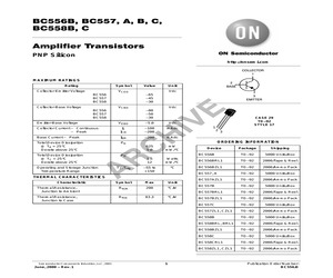
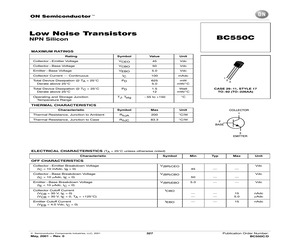
BC558B, C Amplifier Transistors PNP Silicon http://onsemi.com COLLECTOR 1 MAXIMUM RATINGS Rating Symbol Collector-Emitter Voltage Value VCEO BC556 BC557 BC558 Collector-Base Voltage Vdc -65 -45 -30 3 EMITTER VCBO BC556 BC557 BC558 Emitter-Base Voltage Vdc -80 -50 -30 VEBO -5.0 Vdc Collector Current -- Continuous Collector Current -- Peak IC ICM -100 -200 mAdc Base Current -- Peak IBM -200 mAdc Total Device Dissipation @ TA = 25C Derate above 25C PD 625 5.0 mW mW/C Total Device Dissipation @ TC = 25C Derate above 25C PD 1.5 12 Watts mW/C -55 to +150 C Symbol Max Unit Thermal Resistance, Junction to Ambient RJA 200 C/W Thermal Resistance, Junction to Case RJC Operating and Storage Junction Temperature Range TJ, Tstg Semiconductor Components Industries, LLC, 2001 June, 2000 - Rev. 1 CASE 29 TO-92 STYLE 17 1 2 3 ORDERING INFORMATION THERMAL CHARACTERISTICS Characteristic 2 BASE Unit 83.3 C/W 1 Device Package Shipping BC556B TO-92 5000 Units/Box BC556BRL1 TO-92 2000/Tape & Reel BC556BZL1 TO-92 2000/Am
 8 Pages, 117 KB, Original
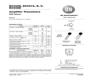
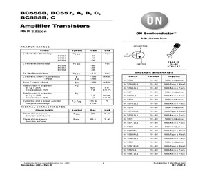
BC558B Amplifier Transistors PNP Silicon http://onsemi.com Features * Pb-Free Packages are Available* COLLECTOR 1 MAXIMUM RATINGS Rating Symbol Collector - Emitter Voltage Value VCEO BC556 BC557 BC558 Collector - Base Voltage Vdc VCBO Vdc -80 -50 -30 VEBO -5.0 Vdc Collector Current - Continuous Collector Current - Peak IC ICM -100 -200 mAdc Base Current - Peak IBM -200 mAdc Total Device Dissipation @ TA = 25C Derate above 25C PD 625 5.0 mW mW/C Total Device Dissipation @ TC = 25C Derate above 25C PD 1.5 12 W mW/C TJ, Tstg -55 to +150 C Characteristic Symbol Max Unit Thermal Resistance, Junction-to-Ambient RqJA 200 C/W Thermal Resistance, Junction-to-Case RqJC 83.3 C/W Operating and Storage Junction Temperature Range 3 EMITTER -65 -45 -30 BC556 BC557 BC558 Emitter - Base Voltage 2 BASE Unit TO-92 CASE 29 STYLE 17 1 12 3 STRAIGHT LEAD BULK PACK 2 3 BENT LEAD TAPE & REEL AMMO PACK MARKING DIAGRAM THERMAL CHARACTERISTICS BC 55xx AYWW G G Stresses exceeding Maximum Ratings may damage the device. Maxim
 10 Pages, 156 KB, Original
8C BC239C BC338-25 MPS4124 - MPS5172 MPS6521 PNP MPSL51 - - - MPS8599 MPSA56 - MPS6729 - BC556B - BC488B MPSA55 MPS2907A 2N5087 BC212 - BC212B - - BC307B BC307C BC327 BC327-16 BC327-25 BC327-40 BC560C BC557 BC557A BC557B BC557C - - - 2N4403 MPS6652 2N3906 BC558B BC558C BC213 - - - - - - - - MPS4126 - MPS6523 V(BR)CEO 100 100 100 80 80 80 80 80 65 65 60 60 60 60 50 50 50 50 45 45 45 45 45 45 45 45 45 45 45 45 45 45 40 40 40 40 40 30 30 30 30 30 25 25 25 25 25 25 25 25 25 IC mA Max Min 600 300 300 500 500 500 250 500 100 100 500 500 500 600 50 100 100 100 100 100 100 100 800 800 800 800 100 100 100 100 100 200 100 600 600 1000 200 100 100 100 600 50 50 100 100 100 800 200 200 100 100 40 50 120 50 100 100 60 50 120 180 60 160 100 100 250 120 120 200 120 120 200 380 100 100 160 250 380 120 120 180 380 500 40 100 100 50 100 200 420 80 100 350 450 200 380 380 160 120 120 100 300 hFE fT Max dB Max 250 460 220 460 300 - 400 250 450 450 400 400 - 300 800 500 260 500 800 220 460 800 630 250 400 630 800 800
 1135 Pages, 16458 KB, Original
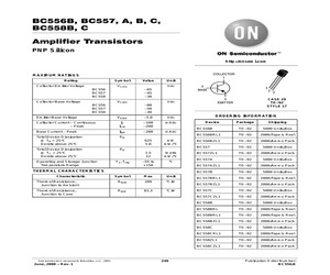
BC558B, C Amplifier Transistors PNP Silicon http://onsemi.com COLLECTOR 1 MAXIMUM RATINGS Rating Symbol Collector-Emitter Voltage Value VCEO BC556 BC557 BC558 Collector-Base Voltage Vdc -65 -45 -30 VCBO BC556 BC557 BC558 Emitter-Base Voltage Unit Vdc Collector Current - Continuous Collector Current - Peak IC ICM -100 -200 mAdc Base Current - Peak IBM -200 mAdc Total Device Dissipation @ TA = 25C Derate above 25C PD Total Device Dissipation @ TC = 25C Derate above 25C PD 625 5.0 mW mW/C 1.5 12 Watts mW/C -55 to +150 C Symbol Max Unit Thermal Resistance, Junction to Ambient RJA 200 C/W Thermal Resistance, Junction to Case RJC 83.3 TJ, Tstg THERMAL CHARACTERISTICS Semiconductor Components Industries, LLC, 2001 June, 2000 - Rev. 1 2 3 EMITTER -80 -50 -30 -5.0 Characteristic 1 Vdc VEBO Operating and Storage Junction Temperature Range 2 BASE C/W 249 3 CASE 29 TO-92 STYLE 17 ORDERING INFORMATION Device Package Shipping BC556B TO-92 5000 Units/Box BC556BRL1 TO-92 2000/Tape & Reel BC556BZL1 TO-92 2000/Amm
 6 Pages, 169 KB, Original
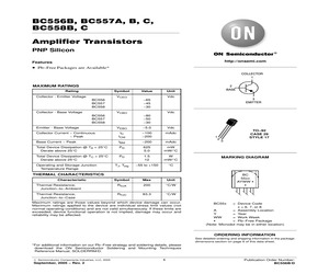
BC558B, C Amplifier Transistors PNP Silicon http://onsemi.com Features * Pb-Free Packages are Available* COLLECTOR 1 MAXIMUM RATINGS Rating Symbol Collector - Emitter Voltage Value VCEO BC556 BC557 BC558 Collector - Base Voltage Vdc VCBO Vdc -80 -50 -30 VEBO -5.0 Vdc IC mAdc ICM -100 -200 Base Current - Peak IBM -200 mAdc Total Device Dissipation @ TA = 25C Derate above 25C PD 625 5.0 mW mW/C Total Device Dissipation @ TC = 25C Derate above 25C PD 1.5 12 W mW/C TJ, Tstg -55 to +150 C Symbol Max Unit Thermal Resistance, Junction-to-Ambient RqJA 200 C/W Thermal Resistance, Junction-to-Case RqJC 83.3 C/W Collector Current - Continuous Collector Current - Peak Operating and Storage Junction Temperature Range 3 EMITTER -65 -45 -30 BC556 BC557 BC558 Emitter - Base Voltage 2 BASE Unit 1 2 TO-92 CASE 29 STYLE 17 3 MARKING DIAGRAM THERMAL CHARACTERISTICS Characteristic Maximum ratings are those values beyond which device damage can occur. Maximum ratings applied to the device are individual stress limit v
 7 Pages, 67 KB, Original
tegy and soldering details, please download the ON Semiconductor Soldering and Mounting Techniques Reference Manual, SOLDERRM/D. Semiconductor Components Industries, LLC, 2004 May, 2004 - Rev. 1 330 Publication Order Number: BC556B/D BC556B, BC557A, B, C, BC558B ELECTRICAL CHARACTERISTICS (TA = 25C unless otherwise noted) Characteristic Symbol Min Typ Max -65 -45 -30 - - - - - - -80 -50 -30 - - - - - - -5.0 -5.0 -5.0 - - - - - - - - - - - - -2.0 -2.0 -2.0 - - - -100 -100 -100 -4.0 -4.0 -4.0 - - - 120 120 180 420 - - - 90 150 270 - 170 290 500 120 180 300 - - - 800 220 460 800 - - - - - - -0.075 -0.3 -0.25 -0.3 -0.6 -0.65 - - -0.7 -1.0 - - -0.55 - -0.62 -0.7 -0.7 -0.82 - - - 280 320 360 - - - - 3.0 6.0 - - - 2.0 2.0 2.0 10 10 10 125 125 240 450 - - - - 900 260 500 900 Unit OFF CHARACTERISTICS Collector -Emitter Breakdown Voltage (IC = -2.0 mAdc, IB = 0) Collector -Base Breakdown Voltage (IC = -100 Adc) Emitter -Base Breakdown Voltage (IE = -100 Adc, IC = 0) Collector-Emitter Leakage Current (VCES
 8 Pages, 241 KB, Original
BC558B, C Amplifier Transistors PNP Silicon http://onsemi.com COLLECTOR 1 MAXIMUM RATINGS Rating Symbol Collector-Emitter Voltage Value Unit VCEO BC556 BC557 BC558 Collector-Base Voltage Vdc -65 -45 -30 VCBO BC556 BC557 BC558 Emitter-Base Voltage Vdc Collector Current - Continuous Collector Current - Peak IC ICM -100 -200 mAdc Base Current - Peak IBM -200 mAdc Total Device Dissipation @ TA = 25C Derate above 25C PD Total Device Dissipation @ TC = 25C Derate above 25C PD 625 5.0 mW mW/C 1.5 12 Watts mW/C -55 to +150 C Symbol Max Unit Thermal Resistance, Junction to Ambient RJA 200 C/W Thermal Resistance, Junction to Case RJC 83.3 TJ, Tstg THERMAL CHARACTERISTICS Semiconductor Components Industries, LLC, 2001 November, 2001- Rev. 0 2 3 EMITTER -80 -50 -30 -5.0 Characteristic 1 Vdc VEBO Operating and Storage Junction Temperature Range 2 BASE C/W 1 3 CASE 29 TO-92 STYLE 17 ORDERING INFORMATION Device Package Shipping BC556B TO-92 5000 Units/Box BC556BRL1 TO-92 2000/Tape & Reel BC556BZL1 TO-92 2000/Am
 8 Pages, 109 KB, Original
BC558B, C Amplifier Transistors PNP Silicon http://onsemi.com COLLECTOR 1 MAXIMUM RATINGS Rating Symbol Collector-Emitter Voltage Value Unit VCEO BC556 BC557 BC558 Collector-Base Voltage Vdc -65 -45 -30 VCBO BC556 BC557 BC558 Emitter-Base Voltage Vdc Collector Current - Continuous Collector Current - Peak IC ICM -100 -200 mAdc Base Current - Peak IBM -200 mAdc Total Device Dissipation @ TA = 25C Derate above 25C PD Total Device Dissipation @ TC = 25C Derate above 25C PD 625 5.0 mW mW/C 1.5 12 Watts mW/C -55 to +150 C Symbol Max Unit Thermal Resistance, Junction to Ambient RJA 200 C/W Thermal Resistance, Junction to Case RJC 83.3 TJ, Tstg THERMAL CHARACTERISTICS Semiconductor Components Industries, LLC, 2001 June, 2000 - Rev. 1 2 3 EMITTER -80 -50 -30 -5.0 Characteristic 1 Vdc VEBO Operating and Storage Junction Temperature Range 2 BASE C/W 1 3 CASE 29 TO-92 STYLE 17 ORDERING INFORMATION Device Package Shipping BC556B TO-92 5000 Units/Box BC556BRL1 TO-92 2000/Tape & Reel BC556BZL1 TO-92 2000/Ammo
 8 Pages, 109 KB, Original
age Marking Convention** BC558 Full Production $0.061 TO-92 3 BULK Line 1: $Y (Fairchild logo) &Z (Asm. Plant Code) &3 (3-Digit Date Code) Line 2: BC558 BC558ABU Full Production $0.0253 TO-92 3 BULK Line 1: BC558 Line 2: A Line 3: -&3 mhtml:file://C:\TEMP\BC558BTAR.mht 16-Aug-2007 Product Folder - Fairchild P/N BC558 - PNP Epitaxial Silicon Transistor BC558ATA Full Production $0.0253 TO-92 Page 2 of 4 3 AMMO Line 1: BC558 Line 2: A Line 3: -&3 BC558B Full Production $0.061 TO-92 3 BULK Line 1: $Y (Fairchild logo) &Z (Asm. Plant Code) &3 (3-Digit Date Code) Line 2: BC Line 3: 558B BC558BBU Full Production $0.0253 TO-92 3 BULK Line 1: BC558 Line 2: B Line 3: -&3 BC558BTA Full Production $0.0253 TO-92 3 AMMO Line 1: BC558 Line 2: B Line 3: -&3 BC558BTAR Full Production $0.0253 TO-92 3 AMMO Line 1: BC558 Line 2: B Line 3: -&3 BC558BTF Full Production $0.0253 TO-92 3 TAPE REEL Line 1: BC558 Line 2: B Line 3: -&3 BC558BTFR Fu
 8 Pages, 184 KB, Original
ersion 1.2P This Material Copyrighted By Philips Semiconductors.BC556 to 558 PHILIPS. INTERNATIONAL 100 7285709 BC557C BC558 Ic (mA) BC556A 557 80 BC558A 0 500 750 1000 = Vag (mV) Fig. 2 Vog = 5 V; Tj = 25 C. 10? lp (uA) BC556A BC557A BC5S8A BC556B BC557B BC558B C557 BCS558C 10 100 0 100 200 T; (C) Fig.4 Vce=5 V: ilo =10mA. Ip (pA) BCSSGA BC557 BC55BA BCS556B BC&57B BC558B BC557 BC558C 10100 0 100 200 T; (OC) Fig.6 Vcop =5 V; Ic =0,1 mA. 162 June 1992 +) ( Printed From CAPS XPert Version 1.2P 7-29-21 5bE >) 2410826 oo4e039 bh mE PHIN 103 (HA) BCSSGA CS57A BC55B8A BC&556B BC557B BC558B BC557 BC558C 10? 100 0 100 7, (01 200 Fig. 3 VceE=5V; Ic =50 mA. 10 ~_ Ip {HA} BCB56A BC557A BC558A B BC557B BC558B BC557C BCS5S58C 1 100 0 100 1, (c) 200 Fig. 5 Vop=5Vilo=1mA, 260 7285708 ve, LL INGE MHz / ack J lessee NO 180 BC558B SIN at AN /\_lecesval IN Bc558ay | STN PN DN a 100 PR 0 50 100 lI fmA) Fig. 7 Vce =5 V; Tj = 25 C; f = 35 MHz. This Material Copyrigh
 6 Pages, 177 KB, Scan
8C BC239C BC338-25 MPS4124 - MPS5172 MPS6521 PNP MPSL51 - - - MPS8599 MPSA56 - MPS6729 - BC556B - BC488B MPSA55 MPS2907A 2N5087 BC212 - BC212B - - BC307B BC307C BC327 BC327-16 BC327-25 BC327-40 BC560C BC557 BC557A BC557B BC557C - - - 2N4403 MPS6652 2N3906 BC558B BC558C BC213 - - - - - - - - MPS4126 - MPS6523 V(BR)CEO 100 100 100 80 80 80 80 80 65 65 60 60 60 60 50 50 50 50 45 45 45 45 45 45 45 45 45 45 45 45 45 45 40 40 40 40 40 30 30 30 30 30 25 25 25 25 25 25 25 25 25 IC mA Max Min 600 300 300 500 500 500 250 500 100 100 500 500 500 600 50 100 100 100 100 100 100 100 800 800 800 800 100 100 100 100 100 200 100 600 600 1000 200 100 100 100 600 50 50 100 100 100 800 200 200 100 100 40 50 120 50 100 100 60 50 120 180 60 160 100 100 250 120 120 200 120 120 200 380 100 100 160 250 380 120 120 180 380 500 40 100 100 50 100 200 420 80 100 350 450 200 380 380 160 120 120 100 300 hFE fT Max dB Max 250 460 220 460 300 - 400 250 450 450 400 400 - 300 800 500 260 500 800 220 460 800 630 250 400 630 800 800
 1135 Pages, 15297 KB, Original
8C BC239C BC338-25 MPS4124 - MPS5172 MPS6521 PNP MPSL51 - - - MPS8599 MPSA56 - MPS6729 - BC556B - BC488B MPSA55 MPS2907A 2N5087 BC212 - BC212B - - BC307B BC307C BC327 BC327-16 BC327-25 BC327-40 BC560C BC557 BC557A BC557B BC557C - - - 2N4403 MPS6652 2N3906 BC558B BC558C BC213 - - - - - - - - MPS4126 - MPS6523 V(BR)CEO 100 100 100 80 80 80 80 80 65 65 60 60 60 60 50 50 50 50 45 45 45 45 45 45 45 45 45 45 45 45 45 45 40 40 40 40 40 30 30 30 30 30 25 25 25 25 25 25 25 25 25 IC mA Max Min 600 300 300 500 500 500 250 500 100 100 500 500 500 600 50 100 100 100 100 100 100 100 800 800 800 800 100 100 100 100 100 200 100 600 600 1000 200 100 100 100 600 50 50 100 100 100 800 200 200 100 100 40 50 120 50 100 100 60 50 120 180 60 160 100 100 250 120 120 200 120 120 200 380 100 100 160 250 380 120 120 180 380 500 40 100 100 50 100 200 420 80 100 350 450 200 380 380 160 120 120 100 300 hFE fT Max dB Max 250 460 220 460 300 - 400 250 450 450 400 400 - 300 800 500 260 500 800 220 460 800 630 250 400 630 800 800
 1135 Pages, 15300 KB, Original
ckage EBIPOLAR.SLB * * BC557AP/ZTX ZETEX.SLB * * BC557B BC557B EBIPOLAR.SLB * * Bipolar Transistor BC557C BC557C EBIPOLAR.SLB * * Bipolar Transistor BC558A BC558A EBIPOLAR.SLB * * Bipolar Transistor BC558AP/ZTX BC558AP/ZTX ZETEX.SLB * * Bipolar Transistor BC558B BC558B EBIPOLAR.SLB * * Bipolar Transistor BC558B/SIE BC558B/SIE SIEMPWR.SLB * * Bipolar Transistor BC558C BC558C EBIPOLAR.SLB * * Bipolar Transistor BC559A BC559A EBIPOLAR.SLB * * Bipolar Transistor BC559AP/ZTX BC559AP/ZTX ZETEX.SLB * * Bipolar Transistor BC559B BC559B EBIPOLAR.SLB * * Bipolar Transistor BC559C BC559C EBIPOLAR.SLB * * Bipolar Transistor BC560A BC560A EBIPOLAR.SLB * * Bipolar Transistor BC560AP/ZTX BC560AP/ZTX ZETEX.SLB * * Bipolar Transistor BC560B BC560B EBIPOLAR.SLB * * Bipolar Transistor BC560C BC560C EBIPOLAR.SLB * * Bipolar Transistor BC807-16 BC807-16 EBIPOLAR.SLB * * Bipolar Transistor BC807-25 BC807-25 EBIPOLAR.SLB * * Bipolar Transistor BC807-40 BC807-40 EBIPOLAR.SLB * * Bi
 573 Pages, 724 KB, Original
BC558B Amplifier Transistors PNP Silicon http://onsemi.com Features * Pb-Free Packages are Available* COLLECTOR 1 MAXIMUM RATINGS Rating Symbol Collector - Emitter Voltage Value VCEO BC556 BC557 BC558 Collector - Base Voltage Vdc VCBO Vdc -80 -50 -30 VEBO -5.0 Vdc Collector Current - Continuous Collector Current - Peak IC ICM -100 -200 mAdc Base Current - Peak IBM -200 mAdc Total Device Dissipation @ TA = 25C Derate above 25C PD 625 5.0 mW mW/C Total Device Dissipation @ TC = 25C Derate above 25C PD 1.5 12 W mW/C TJ, Tstg -55 to +150 C Characteristic Symbol Max Unit Thermal Resistance, Junction-to-Ambient RqJA 200 C/W Thermal Resistance, Junction-to-Case RqJC 83.3 C/W Operating and Storage Junction Temperature Range 3 EMITTER -65 -45 -30 BC556 BC557 BC558 Emitter - Base Voltage 2 BASE Unit TO-92 CASE 29 STYLE 17 1 12 3 STRAIGHT LEAD BULK PACK 2 3 BENT LEAD TAPE & REEL AMMO PACK MARKING DIAGRAM THERMAL CHARACTERISTICS BC 55xx AYWW G G Stresses exceeding Maximum Ratings may damage the device. Maxim
 8 Pages, 85 KB, Original
Z Fairchild BC557 EM 2/2/03 BC557_D74Z Fairchild BC557 EM 2/2/03 BC557B_D27Z Fairchild BC557B EM 2/2/03 BC557B_D74Z Fairchild BC557B EM 2/2/03 BC557B_D75Z Fairchild BC557B EM 2/2/03 BC558_D27Z Fairchild BC558 EM 2/2/03 BC558_D74Z Fairchild BC558 EM 2/2/03 BC558B_D26Z Fairchild BC558B EM 2/2/03 BC558B_D27Z Fairchild BC558B EM 2/2/03 BC558B_D74Z Fairchild BC558B EM 2/2/03 BC558B_D75Z Fairchild BC558B EM 2/2/03 BC558C_D75Z Fairchild BC558C EM 2/2/03 BC559B_D75Z Fairchild BC559B EM 2/2/03 BC559C On Semiconductor (Motorola) BC559C EM BC560C_D74Z Fairchild BC560C EM 2/2/03 BC636_D26Z Fairchild BC636 EM 2/2/03 BC636_D27Z Fairchild BC636 EM 2/2/03 BC636_D74Z Fairchild BC636 EM 2/2/03 BC636_D75Z Fairchild BC636 EM 2/2/03 BC638_D26Z Fairchild BC638 EM 2/2/03 BC638_D27Z Fairchild BC638 EM 2/2/03 2/2/03 2/2/03 2/2/03 2/2/03 5/9/02 BC640_D26Z Fairchild BC640 EM BC640_D27Z Fairchild BC640 EM BC640_D74Z Fairchild BC640 EM
 29 Pages, 82 KB, Original


