stages. The reservoir output capacitor value should be roughly 10 times the value of the flying capacitor. Use larger capacitors for reduced output ripple. positive and negative charge pumps (regardless of the number of stages) is: VREVERSE = VIN - VF The BAT54SDW quad Schottky diode in a SOT363 (2x2mm) package is a good choice for multiple-stage charge pump configuration. White LED Driver The white LED backlight driver can be enabled when input supply rises above under voltage lockout threshold. To reduce inrush current it is recommended that the main boost and white LED driver are not enabled concurrently. Over-Voltage Protection (OVP) with Open Circuit Failure The OVP protection circuit consists of a resistor network tied from the output voltage to the OVP pin (see Figure 3). To protect the device from open circuit failure, the resistor divider can be selected such that the over-voltage threshold occurs prior to the output reaching VLED+(MAX). The value of R5 should be selected from 10k to 20k
 29 Pages, 3438 KB, Original
stages. The reservoir output capacitor value should be roughly 10 times the value of the flying capacitor. Use larger capacitors for reduced output ripple. positive and negative charge pumps (regardless of the number of stages) is: VREVERSE = VIN - VF The BAT54SDW quad Schottky diode in a SOT363 (2x2mm) package is a good choice for multiple-stage charge pump configuration. White LED Driver The white LED backlight driver can be enabled when input supply rises above under voltage lockout threshold. To reduce inrush current it is recommended that the main boost and white LED driver are not enabled concurrently. Over-Voltage Protection (OVP) with Open Circuit Failure The OVP protection circuit consists of a resistor network tied from the output voltage to the OVP pin (see Figure 3). To protect the device from open circuit failure, the resistor divider can be selected such that the over-voltage threshold occurs prior to the output reaching VLED+(MAX). The value of R5 should be selected from 10k to 20k
 28 Pages, 3450 KB, Original
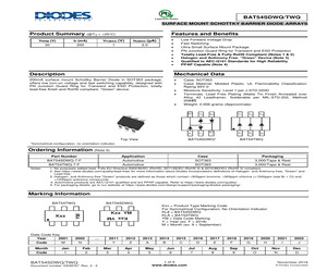
BAT54SDWQ/TWQ SURFACE MOUNT SCHOTTKY BARRIER DIODE ARRAYS Product Summary (@TA = +25C) Features and Benefits VRRM (V) IF (mA) VF(MAX) (V) IR(MAX) (A) 30 200 1 2.0 Low Forward Voltage Drop Fast Switching Ultra-Small Surface Mount Package PN Junction Guard Ring for Transient and ESD Protection Totally Lead-Free & Fully RoHS Compliant (Notes 1 & 2) Halogen and Antimony Free. "Green" Device (Note 3) Qualified to AEC-Q101 Standards for High Reliability PPAP Capable (Note 4) Description Mechanical Data 200mA surface mount Schottky Barrier Diode in SOT363 package, offers low turn-on voltage and fast switching capability, designed with PN Junction Guard Ring for Transient and ESD Protection, totally lead-free finish and RoHS compliant, "Green" device. Case: SOT363 Case Material: Molded Plastic. UL Flammability Classification Rating 94V-0 Moisture Sensitivity: Level 1 per J-STD-020D Terminals: Lead Free Plating (Matte Tin Finish Annealed over Alloy 42 Leadframe). Solderable per MIL-STD-202, Method 208 Wei
 5 Pages, 381 KB, Original
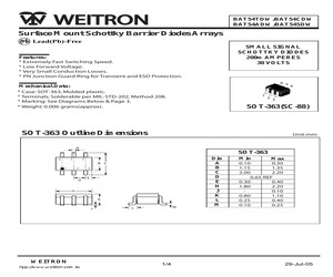
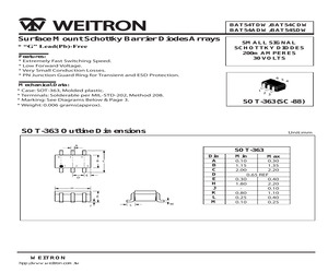
BAT54SDW Surface Mount Schottky Barrier Diodes Arrays SMALL SIGNAL SCHOTTKY DIODES 200m AMPERES 30 VOLTS Features: * Extremely Fast Switching Speed. * Low Forward Voltage. * Very Small Conduction Losses. * PN Junction Guard Ring for Transient and ESD Protection. 6 5 Mechanical Data: * Case: SOT-363, Molded plastic. * Terminals: Solderable per MIL-STD-202, Method 208. * Marking: See Diagrams Below & Page 3. * Weight: 0.006 grams(approx). 1 2 4 3 SOT-363(SC-88) SOT-363 Outline Dimensions Unit:mm A SOT-363 6 5 4 B C 1 2 D 3 E H K J WEITRON hpp://www.weitron.com.tw M L 1/4 Dim A B C D E H J K L M Min Max 0.10 0.30 1.15 1.35 2.00 2.20 0.65 REF 0.30 0.40 1.80 2.20 0.10 0.80 1.10 0.25 0.40 0.10 0.25 29-Jul-05 WEITRON BAT54TDW/BAT54CDW BAT54ADW/BAT54SDW Maximum Ratings (TA=25 C Unless otherwise noted) Symbol Characteristic Peak Repetitive Reverse Voltage Working Peak Reverse Voltage DC Blocking Voltage Unit 30 V IF(AV) 200 mA IFRM 300 mA IFSM 600 mA Pd 200 mw R JA 625 C/W TJ -55 to +125 C Ts
 4 Pages, 479 KB, Original
 shut down all the charge pumps if the die temperature rises above the preset internal thermal limit. This protects the device if the ambient temperature exceeds the operating limit for the device. IN IN OSC DRVN CTL C11 1/2 A3 VIN OSC C12 CTL 1/2 A4 DRVP BAT54SDW BAT54SDW R1 FBN VON = -(R1/R2) x VREF R4 FBP VON R2 GND VREF 1.2V C23 C5 Figure 1: Negative Charge Pump Block Diagram. 10 VOP R4 VOP = 1 + x VREF R3 VREF 1.2V R3 C24 GND Figure 2: Postive Charge Pump Block Diagram. 2820.2006.04.1.4 AAT2820 Triple-Output Charge Pump Regulator Design Procedure and Component Selection Number of Stages for Dual Charge Pump Regulators The number of stages required can be determined by: NPOS = VPOS - 5 5 - 2VFWD for the positive output, and NNEG = VNEG 2VFWD - 5 for the negative output. Where, VNEG = Negative output voltage VPOS = Positive output voltage VFWD = Forward voltage drop of the Schottky diode (0.31V, based on BAT54SDW diode when IF = 4mA) After solving for the number of st
 18 Pages, 441 KB, Original
 shut down all the charge pumps if the die temperature rises above the preset internal thermal limit. This protects the device if the ambient temperature exceeds the operating limit for the device. IN IN C11 1/2 A3 OSC VIN DRVN CTL OSC C12 CTL 1/2 A4 DRVP BAT54SDW BAT54SDW R1 FBN VON = -(R1/R2) x VREF R4 FBP VON R2 C23 VREF 1.2V GND VREF 1.2V R3 C24 C5 Figure 1: Negative Charge Pump Block Diagram. 10 VOP R4 VOP = 1 + x VREF R3 GND Figure 2: Postive Charge Pump Block Diagram. 2820.2005.08.1.2 AAT2820 Triple-Output Charge Pump Regulator Design Procedure and Component Selection Number of Stages for Dual Charge Pump Regulators The number of stages required can be determined by: NPOS = VPOS - 5 5 - 2VFWD for the positive output, and NNEG = VNEG 2VFWD - 5 for the negative output. Where, VNEG = Negative output voltage VPOS = Positive output voltage VFWD = Forward voltage drop of the Schottky diode (0.31V, based on BAT54SDW diode when IF = 4mA) After solving for the number of st
 18 Pages, 346 KB, Original
stages. The reservoir output capacitor value should be roughly 10 times the value of the flying capacitor. Use larger capacitors for reduced output ripple. positive and negative charge pumps (regardless of the number of stages) is: VREVERSE = VIN - VF The BAT54SDW quad Schottky diode in a SOT363 (2x2mm) package is a good choice for multiple-stage charge pump configuration. White LED Driver The white LED backlight driver can be enabled when input supply rises above under voltage lockout threshold. To reduce inrush current it is recommended that the main boost and white LED driver are not enabled concurrently. Over-Voltage Protection (OVP) with Open Circuit Failure The OVP protection circuit consists of a resistor network tied from the output voltage to the OVP pin (see Figure 3). To protect the device from open circuit failure, the resistor divider can be selected such that the over-voltage threshold occurs prior to the output reaching VLED+(MAX). The value of R5 should be selected from 10k to 20k
 28 Pages, 3863 KB, Original
5 SystemPowerTM TFT-LCD DC-DC Converter with WLED Driver and VCOM Buffer 6 is 6.04k. It is best to select the smallest value possible for R10, as this will keep the value of R9 to a minimum. With R10 selected, R9 can be determined: VREVERSE = VIN - VF The BAT54SDW quad Schottky diode in a SOT363 (2x2mm) package is a good choice for multiple-stage charge pump configuration. VGL VGL R9 = V * R10 = 1.2V * R10 REF Positive Output Voltage (VGH) The positive output voltage is set by a resistive divider from the output (VGH) to the FBP and ground pins. Limiting the value of R7 to 6.04k or lower reduces noise in the feedback circuit. Once R7 has been determined, solve for R6: R6 = R7 * number of stages) is: White LED Driver The white LED backlight driver can be enabled when input supply rises above under voltage lockout threshold. To reduce inrush current it is recommended that the main boost and white LED driver are not enabled concurrently. Over-Voltage Protection (OVP) with Open Circuit Failure VGH VG
 28 Pages, 3112 KB, Original
 shut down all the charge pumps if the die temperature rises above the preset internal thermal limit. This protects the device if the ambient temperature exceeds the operating limit for the device. IN IN C11 1/2 A3 OSC VIN DRVN CTL OSC C12 CTL 1/2 A4 DRVP BAT54SDW BAT54SDW R1 FBN VON = -(R1/R2) x VREF R4 FBP VON R4 VOP = 1 + x VREF R3 R2 VREF 1.2V C23 VREF 1.2V GND C5 R3 C24 GND Figure 1: Negative Charge Pump Block Diagram. 10 VOP Figure 2: Postive Charge Pump Block Diagram. www.analogictech.com 2820.2010.04.1.5 PRODUCT DATASHEET AAT2820 ChargePumpTM Triple-Output Charge Pump Regulator Design Procedure and Component Selection Number of Stages for Dual Charge Pump Regulators The number of stages required can be determined by: NPOS = VPOS - 5 5 - 2VFWD for the positive output, and NNEG = VNEG 2VFWD - 5 for the negative output. Where, VNEG = Negative output voltage VPOS = Positive output voltage VFWD = Forward voltage drop of the Schottky diode (0.31V, based on BAT54SDW dio
 17 Pages, 761 KB, Original
supply rises above under voltage lockout threshold. To reduce inrush current it is recommended that the main boost and white LED driver are not enabled concurrently. Once R7 has been determined, solve for R6: VGH VGH - 1 = R7 * -1 VREF 0.6V R6 = R 7 * The BAT54SDW quad Schottky diode in a SOT363 (2x2mm) package is a good choice for multiple-stage charge pump configuration. Flying and Output Capacitors The minimum value for the flying capacitor is limited by the output power requirement, while the maximum value is set by the bandwidth of the power supply. If CFLY is too small, the output may not be able to deliver the power demanded, while too large of a capacitor may limit the bandwidth and time required to recover from load and line transients. A 0.1F X7R or X5R ceramic capacitor is typically used. The voltage rating of the flying and reservoir output capacitors varies with the number of charge pump stages. The reservoir output capacitor value should be roughly 10 times the value of the flying c
 28 Pages, 531 KB, Original
 shut down all the charge pumps if the die temperature rises above the preset internal thermal limit. This protects the device if the ambient temperature exceeds the operating limit for the device. IN IN C11 1/2 A3 OSC VIN DRVN CTL OSC C12 CTL 1/2 A4 DRVP BAT54SDW BAT54SDW R1 FBN VON = -(R1/R2) x VREF R4 FBP VON R2 C23 VREF 1.2V GND VREF 1.2V R3 C24 C5 Figure 1: Negative Charge Pump Block Diagram. 10 VOP R4 VOP = 1 + x VREF R3 GND Figure 2: Postive Charge Pump Block Diagram. 2820.2005.11.1.3 AAT2820 Triple-Output Charge Pump Regulator Design Procedure and Component Selection Number of Stages for Dual Charge Pump Regulators The number of stages required can be determined by: NPOS = VPOS - 5 5 - 2VFWD for the positive output, and NNEG = VNEG 2VFWD - 5 for the negative output. Where, VNEG = Negative output voltage VPOS = Positive output voltage VFWD = Forward voltage drop of the Schottky diode (0.31V, based on BAT54SDW diode when IF = 4mA) After solving for the number of st
 18 Pages, 312 KB, Original
rvoir capacitor C10. If the voltage across C10 minus a diode drop is less than the voltage across C7, current flows from C7 to C10 until the diode turns off. 3190.2005.03.1.0 AAT3190 Positive/Negative Charge Pump for Voltage Bias IN OSC DRVN CTL C7 1/2 A4 BAT54SDW R1 FBN VON = -(R1/R2) x VREF VON R2 C10 VREF 1.2V AAT3190 C2 GND Figure 1: Negative Charge Pump Block Diagram. MOSFET turns on, level shifting C4 by the input voltage. This connects C4 in parallel with the reservoir capacitor C5. If the voltage across C5 plus a diode drop is less than the level shifted flying capacitor (C4 + VIN), charge is transferred from C4 to C5 until the diode turns off. Positive Charge Pump During the first half-cycle, the N-channel MOSFET turns on and charges the flying capacitor C4 (Figure 2). During the second half-cycle, the Nchannel MOSFET turns off and the P-channel IN VIN OSC C4 CTL 1/2 A3 DRVP BAT54SDW R3 FBP VOP VOP = (1+R3/R4) x VREF VREF 1.2V AAT3190 R4 C5 GND Figure 2: Positive Charge Pump
 16 Pages, 409 KB, Original
BAT54SDW Surface Mount Schottky Barrier Diodes Arrays SMALL SIGNAL SCHOTTKY DIODES 200m AMPERES 30 VOLTS * "G" Lead(Pb)-Free Features: * Extremely Fast Switching Speed. * Low Forward Voltage. * Very Small Conduction Losses. * PN Junction Guard Ring for Transient and ESD Protection. 6 5 Mechanical Data: * Case: SOT-363, Molded plastic. * Terminals: Solderable per MIL-STD-202, Method 208. * Marking: See Diagrams Below & Page 3. * Weight: 0.006 grams(approx). 1 2 3 SOT-363(SC-88) SOT-363 Outline Dimensions Unit:mm A SOT-363 6 5 4 B C 1 2 D 3 E H K J WEITRON hpp://www.weitron.com.tw L 4 M Dim A B C D E H J K L M Min Max 0.10 0.30 1.15 1.35 2.00 2.20 0.65 REF 0.30 0.40 1.80 2.20 0.10 0.80 1.10 0.25 0.40 0.10 0.25 WE IT R ON BAT54TDW/BAT54CDW BAT54ADW/BAT54SDW Maximum Ratings (TA=25 C Unless otherwise noted) Symbol Characteristic Peak Repetitive Reverse Voltage Working Peak Reverse Voltage DC Blocking Voltage Unit 30 V IF(AV) 200 mA IFRM 300 mA IFSM 600 mA Pd 200 mw R JA 625 C/W TJ -55 to
 4 Pages, 101 KB, Original
BAT54SDW Surface Mount Schottky Barrier Diodes Arrays * "G" Lead(Pb)-Free Features: * Extremely Fast Switching Speed. * Low Forward Voltage. * Very Small Conduction Losses. * PN Junction Guard Ring for Transient and ESD Protection. SMALL SIGNAL SCHOTTKY DIODES 200m AMPERES 30 VOLTS 6 5 Mechanical Data: * Case: SOT-363, Molded plastic. * Terminals: Solderable per MIL-STD-202, Method 208. * Marking: See Diagrams Below & Page 3. * Weight: 0.006 grams(approx). 1 2 3 SOT-363(SC-88) SOT-363 Outline Dimensions Unit:mm A SOT-363 6 5 4 B C 1 2 D 3 E H K J WEITRON hpp://www.weitron.com.tw L 4 M Dim A B C D E H J K L M Min Max 0.10 0.30 1.15 1.35 2.00 2.20 0.65 REF 0.30 0.40 1.80 2.20 0.10 0.80 1.10 0.25 0.40 0.10 0.25 WE IT R ON BAT54TDW/BAT54CDW BAT54ADW/BAT54SDW Maximum Ratings (TA=25 C Unless otherwise noted) Symbol Characteristic Peak Repetitive Reverse Voltage Working Peak Reverse Voltage DC Blocking Voltage Unit 30 V IF(AV) 200 mA IFRM 300 mA IFSM 600 mA Pd 200 mw R JA 625 C/W TJ -55 to
 4 Pages, 101 KB, Original
se (Note 3) Lead Free Plating (Matte Tin Finish annealed over Alloy 42 Leadframe). Weight: 0.006 grams (Approximate) Top View UL Flammability Classification Rating 94V-0 A1 C2 C2 C1 A2 A2 AC C1 C1 A2 A1 A1 C2 A1 BAT54ADW* 1 BAT54CDW* AC A2 C2 1 AC C1 A1 2 BAT54SDW* C1 C2 C1 C2 C3 A2 AC A1 A2 A3 2 BAT54BRW BAT54TW *Symmetrical configuration, no orientation indicator. Ordering Information (Note 4) Part Number BAT54ADW-7-F BAT54CDW-7-F BAT54SDW-7-F BAT54BRW-7-F BAT54TW-7-F Notes: Case SOT-363 SOT-363 SOT-363 SOT-363 SOT-363 Packaging 3,000/Tape & Reel 3,000/Tape & Reel 3,000/Tape & Reel 3,000/Tape & Reel 3,000/Tape & Reel 1. No purposely added lead. Fully EU Directive 2002/95/EC (RoHS) & 2011/65/EU (RoHS 2) compliant. 2. See http://www.diodes.com/quality/lead_free.html for more information about Diodes Incorporated's definitions of Halogen- and Antimony-free, "Green" and Lead-free. 3. Halogen- and Antimony-free "Green" products are defined as those which contain <900ppm bromine, <900ppm
 5 Pages, 299 KB, Original


