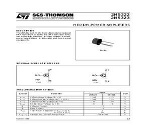
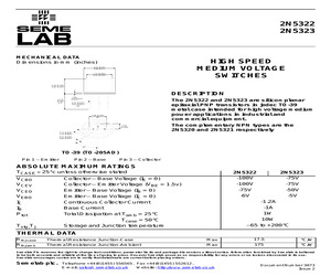
2N5322 2N5323 MEDIUM-POWER AMPLIFIERS DESCRIPTION The 2N5322 and 2N5323 are silicon planar epitaxial PNP transistors in Jedec TO-39 metal case. They are especially intended for high-voltage medium power applications in industrial and commercial equipments. TO-39 INTERNAL SCHEMATIC DIAGRAM ABSOLUTEMAXIMUM RATINGS Symbol Parameter Value 2N5322 2N5323 Unit V CBO Collector-base Voltage (I E = 0) - 100 - 75 V V CEV Collector-emitter Voltage (V B E = 1.5 V) - 100 - 75 V V CEO Collector-emitter Voltage (I B = 0) - 75 - 50 V V EBO Emitter-base Voltage (I C = 0) -6 -5 V IC Collector Current -2 A IB Base Current -1 A Total Power Dissipation at T am b 25 C at T cas e 25 C 1 10 W W - 65 to 200 C Pto t T st g , T j October 1988 Storage and Junction Temperature 1/4 2N5322-2N5323 THERMAL DATA R t h j- cas e R t h j-amb Thermal Resistance Junction-case Thermal Resistance Junction-ambient Max Max C/W C/W 17.5 175 ELECTRICAL CHARACTERISTICS(T case = 25 C unless otherwise spec
 4 Pages, 51 KB, Original
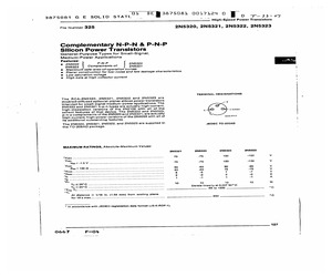
2N5322, 2N5323 Complementary N-P-N & P-N-P Silicon Power Transistors General-Purpose Types for Small-Signal, Medium-Power Applications Features: = 2N5322 P-N-P 2N5320 2N5323 Complements of: 2N5321 = Maximum safe-area-of-operation curves i = Planar construction for iow-noise and low leakage characteristics : = Low saturation voltage : = High beta at high collector current i | TERMINAL DESIGNATIONS | The RCA-2N5320, 2N5321, 2N5322 and 2N5323 are doubled-diffused epltaxial-planar silicon power transistors intended for small-signal medium-power applications. The 2N5320 and 2N5321 n-p-n types are actually high-current, high-dissipation versions of the 2N2102 with all of the | | salient features of that device. The 2N5322 and 2N5323, e (CASED p-n-p complements of the 2N5320 and 2N5321, are actually high-current, high-power versions of the 2N4036 with all of 92c$-27512 its additional outstanding features. ' The 2N5320, 2N5321, 2N5322, and 2N5323 are su
 5 Pages, 232 KB, Scan
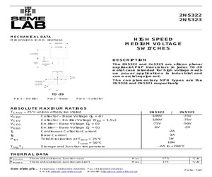
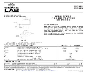
2N5322 2N5323 MECHANICAL DATA Dimensions in mm (inches) HIGH SPEED MEDIUM VOLTAGE SWITCHES 8.89 (0.35) 9.40 (0.37) 7.75 (0.305) 8.51 (0.335) 6.10 (0.240) 6.60 (0.260) DESCRIPTION 12.70 (0.500) min. 0.89 max. (0.035) The 2N5322 and 2n5323 are silicon planar expitaxial PNP transistors in jedec TO-39 metal case intended for high voltage medium power applications in industrial and commercial equipment. 0.41 (0.016) 0.53 (0.021) dia. 5.08 (0.200) typ. 2.54 (0.100) 2 1 3 The complementary NPN types are the 2N5320 and 2N5321 respectively 0.66 (0.026) 1.14 (0.045) 0.71 (0.028) 0.86 (0.034) 45 TO-39 Pin 1 - Emitter Pin 2 - Base Pin 3 - Collector ABSOLUTE MAXIMUM RATINGS TCASE = 25c unless otherwise stated VCBO VCEV VCEO VEBO IC IB Ptot 2N5322 -100V -100V -75V -6V Collector - Base Voltage (IE = 0) Collector - Emitter Voltage (VBE = 1.5v) Emitter - Base Voltage (IB = 0) Emitter - Base Voltage (IC = 0) Continuous Collector Current Base Current Total Dissipation at Tamb = 25C Tcase =
 3 Pages, 39 KB, Original
2N5322 2N5323 MECHANICAL DATA Dimensions in mm (inches) HIGH SPEED MEDIUM VOLTAGE SWITCHES 8 .8 9 (0 .3 5 ) 9 .4 0 (0 .3 7 ) 7 .7 5 (0 .3 0 5 ) 8 .5 1 (0 .3 3 5 ) 6 .1 0 (0 .2 4 0 ) 6 .6 0 (0 .2 6 0 ) 1 2 .7 0 (0 .5 0 0 ) m in . DESCRIPTION 0 .8 9 m a x . (0 .0 3 5 ) The 2N5322 and 2n5323 are silicon planar expitaxial PNP transistors in jedec TO-39 metal case intended for high voltage medium power applications in industrial and commercial equipment. 0.41 (0.016) 0.53 (0.021) d ia . 5 .0 8 (0 .2 0 0 ) ty p . 1 2 3 2 .5 4 (0 .1 0 0 ) The complementary NPN types are the 2N5320 and 2N5321 respectively 0 .6 6 (0 .0 2 6 ) 1 .1 4 (0 .0 4 5 ) 0 .7 1 (0 .0 2 8 ) 0 .8 6 (0 .0 3 4 ) 4 5 TO-39 Pin 1 - Emitter Pin 2 - Base Pin 3 - Collector ABSOLUTE MAXIMUM RATINGS TCASE = 25c unless otherwise stated VCBO VCEV VCEO VEBO IC IB Ptot 2N5322 -100V -100V -75V -6V Collector - Base Voltage (IE = 0) Collector - Emitter Voltage (VBE = 1.5v) Emitter - Base Voltage (IB = 0) Emitter - Base Volta
 2 Pages, 42 KB, Original
2N5322 - 2N5323 SILICON PLANAR EPITAXIAL TRANSISTORS The 2N5322 and 2N5323 are PNP transistors mounted in TO-39 metal case . They are especially intended for high-voltage medium power applications in industrial and commercial equipements. Compliance to RoHS ABSOLUTE MAXIMUM RATINGS Symbol Ratings VCEO Collector-Emitter Voltage (IB = 0) VCBO Collector-Base Voltage (IE = 0) VCEV Collector-Emitter Voltage (VBE = 1.5V) VEBO Emitter-Base Voltage (IC = 0) IC Collector Current IB Base Current PD Total Power Dissipation @ Tamb = 25 @ Tcase= 25 TJ Junction Temperature TStg Storage Temperature range Value 2N5322 2N5323 2N5322 2N5323 2N5322 2N5323 2N5322 2N5323 2N5322 2N5323 2N5322 2N5323 2N5322 2N5323 2N5322 2N5323 2N5322 2N5323 2N5322 2N5323 Unit -75 -50 -100 -75 -100 -75 -6 -5 V V V V -2 A -1 A 1 Watts 10 -65 to +200 C -65 to +200 C THERMAL CHARACTERISTICS Symbol
 3 Pages, 178 KB, Original
2N5322, 2N5323 Complementary N-P-N & P-N-P Silicon Power Transistors General-Purpose Types for Small-Signal, Medium-Power Applications Features: = 2N5322 P-N-P 2N5320 2N5323 Complements of: 2N5321 Maximum safe-area-of-operation curves i Planar construction for low-noise and low leakage characteristics : Low saturation voltage ' High beta at high collector current i TERMINAL DESIGNATIONS The RCA-2N5320, 2N5321, 2N5322 and 2N5323 are doubled-diffused epitaxial-planar silicon power transistors intended for small-signal medium-power applications. The 2N5320 and 2N5321 n-p-n types are actually high-current, high-dissipation versions of the 2N2102 with all of the salient features of that device. The 2N5322 and 2N5323, E (CASE) | p-n-p complements of the 2N5320 and 2N5321, are actually high-current, high-power versions of the 2N4036 with all of 9208-27512 its additional outstanding features. i The 2N5320, 2N5321, 2N5322, and 2N5323 are supplied in JEDE
 5 Pages, 361 KB, Scan
2N5322, 2N5323 HARRIS SEMICOND SECTOR Cee Dd = uadee sh GOu5aES b MEHAS Cc | t N-P-N & P-N-P 1338-07 omplementary N-P- -N- Silicon Power Transistors w 1 O57 1 General-Purpose Types for Small-Signal, Medium-Power Applications Features: = 2N5322 P-N-P 2N5320 2N5323 Complements of: 2N5321 Maximum safe-area-of-operation curves Planar construction for low-noise and low leakage characteristics , a. Low saturation voltage - some ca High beta at high collector current - TERMINAL DESIGNATIONS The 2N5320, 2N5321, 2N5322 and 2N5323 are doubled-diffused epitaxial-planar silicon power transistors intended for small-signal medium-power applications. The 8 2N5320 and 2N5321 n-p-n types are actually high-current, . high-dissipation versions of the 2N2102 with ail of the salient features of that device. The 2N5322 and 2N5323, E CICASED p-n-p complements of the 2N5320 and 2N5321, are actually . . . high-current, high-power versions of the 2N4036 with all of 9208-27512 . its a
 5 Pages, 387 KB, Scan
2N5322 2N5323 SMALL SIGNAL PNP TRANSISTORS SILICON EPITAXIAL PLANAR PNP TRANSISTORS MEDIUM POWER AMPLIFIER NPN COMPLEMENTS ARE 2N5320 AND 2N5321 DESCRIPTION The 2N5322 and 2N5323 are silicon epitaxial planar PNP transistors in Jedec TO-39 metal case. They are especially intended for high-voltage medium power application in industrial and commercial equipments. The complementary NPN types are respectively the 2N5320 and 2N5321 TO-39 INTERNAL SCHEMATIC DIAGRAM ABSOLUTE MAXIMUM RATINGS Symbol Parameter Value 2N5322 Unit 2N5323 V CBO Collector-Base Voltage (I E = 0) -100 -75 V V CEV Collector-Emitter Voltage (V BE = -1.5V) -100 -75 V V CEO Collector-Emitter Voltage (I B = 0) -75 -50 V V EBO Emitter-Base Voltage (I C = 0) -6 -5 V IC I CM IB Collector Current -2 A Base Current -1 A Total Dissipation at T amb = 25 o C P tot Total Dissipation at T c = 25 o C June 1997 A Collector Peak Current P tot T stg , T j -1.2 Storage and Junction Temperature 1 W 10 W -65 to 200 o C 1/4 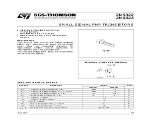 4 Pages, 45 KB, Original
4 Pages, 45 KB, Original2N5322 2N5323 SMALL SIGNAL PNP TRANSISTORS SILICON EPITAXIAL PLANAR PNP TRANSISTORS MEDIUM POWER AMPLIFIER NPN COMPLEMENTS ARE 2N5320 AND 2N5321 DESCRIPTION The 2N5322 and 2N5323 are silicon epitaxial planar PNP transistors in Jedec TO-39 metal case. They are especially intended for high-voltage medium power application in industrial and commercial equipments. The complementary NPN types are respectively the 2N5320 and 2N5321 TO-39 INTERNAL SCHEMATIC DIAGRAM ABSOLUTE MAXIMUM RATINGS Symbol Parameter Value Uni t 2N5322 2N5323 V CBO Collector-Base Voltage (IE = 0) -100 -75 V V CEV Collector-Emitter Voltage (V BE = -1.5V) -100 -75 V V CEO Collector-Emitter Voltage (I B = 0) -75 -50 V V EBO Emitter-Base Voltage (I C = 0) -6 -5 IC I CM IB Collector Current A Collector Peak Current -2 A Base Current -1 A o P t ot Total Dissipation at T amb = 25 C P t ot Total Dissipation at T c = 25 C T stg, T j June 1997 V -1.2 o Storage and Junction Temperature 1 W 10 W -65 to 200 o C 1/4 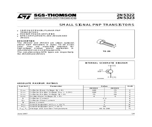 4 Pages, 34 KB, Original
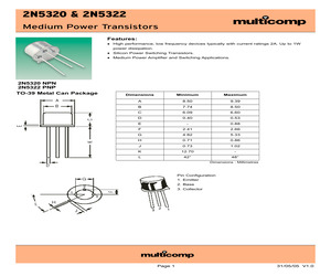
4 Pages, 34 KB, Original2N5322 Medium Power Transistors Features: * High performance, low frequency devices typically with current ratings 2A. Up to 1W power dissipation. * Silicon Power Switching Transistors. * Medium Power Amplifier and Switching Applications. 2N5320 NPN 2N5322 PNP TO-39 Metal Can Package Dimensions Minimum Maximum A 8.50 9.39 B 7.74 8.50 C 6.09 6.60 D 0.40 0.53 E - 0.88 F 2.41 2.66 G 4.82 5.33 H 0.71 0.86 J 0.73 1.02 K 12.70 - L 42 48 Dimensions : Millimetres Pin Configuration 1. Emitter 2. Base 3. Collector Page 1 31/05/05 V1.0 2N5320 & 2N5322 Medium Power Transistors Absolute Maximum Ratings Description 2N5320 NPN 2N5322 PNP Symbol Collector Emitter Voltage VCEO 75 Collector Base Voltage VCBO 100 Emitter Base Voltage VEBO 7 Collector Current-Continuous IC 2.0 Base Current IB 1.0 Power Dissipation at Ta = 25C Derate above 25C Power Dissipation at Tc = 25C Derate above 25C V A 1 5.71 PD Operating and Storage Junction Temperature Range Units W mW/C 10 57.14 Tj, T
 4 Pages, 312 KB, Original
0P | 95/145 | 500mA | RMS| FCD | BSSt6 2N5320 2N5321-V NS | TOS | Los |75v | 5oVv BV | 2A 200C | 1WE 50M 20P | 125mn | 500mA | RMS| FCD | BSS16 2N5320 2N5321-W Ns | Tos | to4 | 75v | sov BV ]2A 200C | 1WE 50M 20P | 165mn | 500mA | RMS | FCD | 8SS16 2N5320 2N5322 PS | TO39 | Los | 100vV | 7ev | 7v [2A 200C | 1WF 50M - 30/130 | 500MA | AMH| STM | BSS17 2N5322 2N5322-R PS | To39 | Los | 100v | JV | 7 [2A 200 | 1WE 50M 40P | 33/50 500mA | RMS | FCD | BSS17 2N4036 2N5322-BR PS | Toss | Loa | 100v | yev | 7 j2A8 200c | 1we 50M 4oP | 25/38 s00mA | RMS! FCD | BSS17 2N4036 2N5322-0 Ps | To39 | Loa | 100v | 75V | FV | 2A 200C | 1WE 50M 4oP | 43/65 500mA | RMS | FCD | BSS17 2N4036 2N5322- Ps | To39 | Loa | 100v | 75V Ww }2A 200C | 1WF 50M 40P | 56/85 500mA | RMS | FCO | BSS17 2N4036 2N5322-GN | PS | TO39 | Loa | 100V | 75v Ww |2A0 200C | 1WF 20M 4oP | 73/100 | 500mA | RMS | FCD | BSS17 2N4036 2N5322-BL PS | TO39 | Los
 1 Pages, 85 KB, Scan
2N5322 2N5323 MECHANICAL DATA Dimensions in mm (inches) HIGH SPEED MEDIUM VOLTAGE SWITCHES 8.51 (0.34) 9.40 (0.37) 7.75 (0.305) 8.51 (0.335) 6.10 (0.240) 6.60 (0.260) DESCRIPTION 12.70 (0.500) min. 0.89 max. (0.035) The 2N5322 and 2N5323 are silicon planar epitaxial PNP transistors in jedec TO-39 metal case intended for high voltage medium power applications in industrial and commercial equipment. 0.41 (0.016) 0.53 (0.021) dia. 5.08 (0.200) typ. 2.54 (0.100) 2 1 3 The complementary NPN types are the 2N5320 and 2N5321 respectively 0.74 (0.029) 1.14 (0.045) 0.71 (0.028) 0.86 (0.034) 45 TO-39 (TO-205AD) Pin 1 - Emitter Pin 2 - Base Pin 3 - Collector ABSOLUTE MAXIMUM RATINGS TCASE = 25c unless otherwise stated VCBO VCEV VCEO VEBO IC IB Ptot 2N5322 -100V -100V -75V -6V Collector - Base Voltage (IE = 0) Collector - Emitter Voltage (VBE = 1.5v) Emitter - Base Voltage (IB = 0) Emitter - Base Voltage (IC = 0) Continuous Collector Current Base Current Total Dissipation at Tamb = 2
 2 Pages, 17 KB, Original
2N5322 2N5323 MECHANICAL DATA Dimensions in mm (inches) HIGH SPEED MEDIUM VOLTAGE SWITCHES 8.89 (0.35) 9.40 (0.37) 7.75 (0.305) 8.51 (0.335) 6.10 (0.240) 6.60 (0.260) DESCRIPTION 12.70 (0.500) min. 0.89 max. (0.035) The 2N5322 and 2n5323 are silicon planar expitaxial PNP transistors in jedec TO-39 metal case intended for high voltage medium power applications in industrial and commercial equipment. 0.41 (0.016) 0.53 (0.021) dia. 5.08 (0.200) typ. 2.54 (0.100) 2 1 3 The complementary NPN types are the 2N5320 and 2N5321 respectively 0.66 (0.026) 1.14 (0.045) 0.71 (0.028) 0.86 (0.034) 45 TO-39 Pin 1 - Emitter Pin 2 - Base Pin 3 - Collector ABSOLUTE MAXIMUM RATINGS TCASE = 25c unless otherwise stated VCBO VCEV VCEO VEBO IC IB Ptot 2N5322 -100V -100V -75V -6V Collector - Base Voltage (IE = 0) Collector - Emitter Voltage (VBE = 1.5v) Emitter - Base Voltage (IB = 0) Emitter - Base Voltage (IC = 0) Continuous Collector Current Base Current Total Dissipation at Tamb = 25C Tcase =
 2 Pages, 35 KB, Original
2N5322 2N5323 MECHANICAL DATA Dimensions in mm (inches) HIGH SPEED MEDIUM VOLTAGE SWITCHES 8.51 (0.34) 9.40 (0.37) 7.75 (0.305) 8.51 (0.335) 6.10 (0.240) 6.60 (0.260) DESCRIPTION 12.70 (0.500) min. 0.89 max. (0.035) The 2N5322 and 2N5323 are silicon planar epitaxial PNP transistors in jedec TO-39 metal case intended for high voltage medium power applications in industrial and commercial equipment. 0.41 (0.016) 0.53 (0.021) dia. 5.08 (0.200) typ. 2.54 (0.100) 2 1 3 The complementary NPN types are the 2N5320 and 2N5321 respectively 0.74 (0.029) 1.14 (0.045) 0.71 (0.028) 0.86 (0.034) 45 TO-39 (TO-205AD) Pin 1 - Emitter Pin 2 - Base Pin 3 - Collector ABSOLUTE MAXIMUM RATINGS TCASE = 25c unless otherwise stated VCBO VCEV VCEO VEBO IC IB Ptot 2N5322 -100V -100V -75V -6V Collector - Base Voltage (IE = 0) Collector - Emitter Voltage (VBE = 1.5v) Emitter - Base Voltage (IB = 0) Emitter - Base Voltage (IC = 0) Continuous Collector Current Base Current Total Dissipation at Tamb = 2
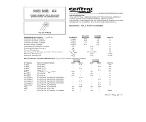
 2 Pages, 16 KB, Original
2N5322 2N5323 NPN PNP COMPLEMENTARY SILICON SWITCHING TRANSISTORS w w w. c e n t r a l s e m i . c o m DESCRIPTION: The CENTRAL SEMICONDUCTOR 2N5320, 2N5322 series types are complementary silicon power transistors manufactured by the epitaxial planar process, designed for amplifier and switching applications. MARKING: FULL PART NUMBER TO-39 CASE MAXIMUM RATINGS: (TC=25C) Collector-Base Voltage Collector-Emitter Voltage Collector-Emitter Voltage Emitter-Base Voltage Continuous Collector Current Continuous Base Current Power Dissipation Operating and Storage Junction Temperature Thermal Resistance Thermal Resistance SYMBOL VCBO VCEV VCEO VEBO IC IB PD TJ, Tstg JA JC 2N5320 2N5322 100 100 75 6.0 ELECTRICAL CHARACTERISTICS: (TC=25C unless otherwise noted) 2N5320 2N5322 SYMBOL TEST CONDITIONS MIN MAX ICBO VCB=80V 0.5 ICBO VCB=60V IEBO VEB=5.0V 0.1 IEBO VEB=4.0V BVCEV IC=100A, VBE=1.5V 100 BVCEO IC=10mA 75 BVEBO IE=100A 6.0 VCE(SAT) IC=500mA, IB=50mA (2N5320) 0.5
 3 Pages, 322 KB, Original


